News Posts matching #Manufacturing

Return to Keyword Browsing

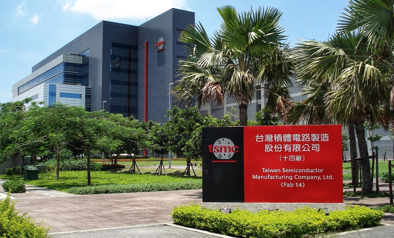
Apple is Reportedly Working with TSMC on a Special Micro OLED Panel Technology

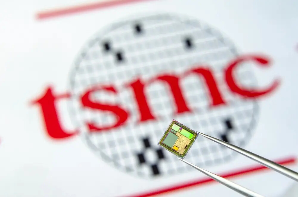
OLED panes are expertise areas of display makers such as LG and Samsung, however, when it comes to Apple, they have to rely on external manufacturers to make a display. For years Apple has been contracting LG and Samsung to make the display for iPhones and Macs, but it looks like Apple is now collaborating with another firm to develop micro OLED technology. According to sources over at Nikkei Asia, Apple is collaborating with Taiwan Semiconductor Manufacturing Company (TSMC) to develop "ultra-advanced display technology at a secretive facility in Taiwan". Despite TSMC not being the traditional choice for panel manufacturing, there is a list of reasons why Apple chose its years-long partner to work with.

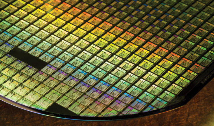
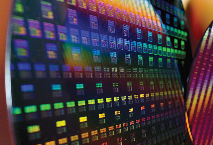
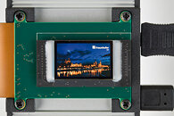
TSMC is known for manufacturing silicon chips, however, Apple envisions that the Taiwan maker will manufacture ultra-advanced micro OLED technology using wafers. Building the displays using wafers will result in much lower power consumption and far lower size. Why is this approach necessary you might wonder? Well, Apple is developing a new generation of AR glasses and there needs to be a solid display technology for them to exist. It is reported that the new micro OLED displays are under development and are about one inch in diameter. The source also adds that this is just one out of two projects being worked on inside of Apple's secretive labs located in the Taiwanese city of Taoyuan. What is the other project remains a mystery, however, with more time we could get information on that as well.

Intel Invests Additional $475 Million in Vietnam

Intel Corporation today announced it has invested a further US $475 million in Intel Products Vietnam (IPV). This new investment is in addition to Intel's US$1 billion investment to build a state-of-the-art chip assembly and test manufacturing facility in Saigon Hi-Tech Park (SHTP), first announced in 2006. This takes Intel's total investment in its Vietnam facility to US $1.5 billion.

"As of the end of 2020, Intel Products Vietnam has shipped more than 2 billion units to customers worldwide. We're very proud of this milestone, which shows both how important IPV is to helping Intel meet the needs of its customers all around the world, and why we continue to invest in our facilities and team here in Vietnam," said Kim Huat Ooi, vice president of Manufacturing and Operations and general manager of Intel Products Vietnam Co. Ltd.

Intel Expands 10nm Manufacturing Capacity

In response to incredible customer demand, Intel has doubled its combined 14 nm and 10 nm manufacturing capacity over the past few years. To do this, the company found innovative ways to deliver more output within existing capacity through yield improvement projects and significant investments in capacity expansion. This video recounts that journey, which even included re-purposing existing lab and office space for manufacturing.

"Over the last three years, we have doubled our wafer volume capacity, and that was a significant investment. Moving forward, we're not stopping… We are continuing to invest into factory capacity to ensure we can keep up with the growing needs of our customers," says Keyvan Esfarjani, senior vice president and general manager of Manufacturing and Operations at Intel. The company also ramped its new 10 nm process this year. Intel currently manufactures 10 nm products in high volumes at its Oregon and Arizona sites in the U.S. and its site in Israel.

Intel's Manufacturing Outlook for the Future Doesn't Inspire Confidence in Successful Competition, According to Susquehanna Call

Susquehanna is a global trading firm which has various interests in silicon manufacturing - and part of that interest is naturally materialized in Intel. In a recent group call from the firm, some details on Intel's manufacturing and product design woes came to light, which point towards even more execution slips than we've already seen. During the call, a number of points were broached, including dismal yields for Intel's 10 nm manufacturing process as of its introduction in late 2018 (which is why it never saw mainstream adoption from the company). News that Intel is looking for a new CEO also don't instill confidence on current CEO Bob Swan's capacity to steer the Intel behemoth.

Improved yields on 10 nm are being reported due to deployment of Intel's SuperFin technology, which improved yields to upwards of 50%, but still keeps them under the ones achieved in Intel's 14 nm process; an eye-opening tidbit in that Cannon Lake on 10 nm originally saw yields of only 25% usable chips per wafer; and that backporting Rocket Lake meant Intel had to deal with unfathomably large chips and high power consumption characteristics. And to add insult to injury, there is still not a definite timetable for 7 nm deployment, with delays being expected to be worse than the previously reported 6-12 months. This all paints a somewhat grim picture for Intel's capacity to compete with TSMC-powered AMD in many of its most important markets; the blue giant won't topple, of course, but it's expected that five years from now, we'll be looking at a very different outlook in the market between AMD and Intel. You can check the talked-about points in the call via the transcript after the break. You should still take the transcript with a grain of salt.

TSMC to Roll Out 3nm Plus Manufacturing Process in 2023

The possibility barely exists to account for all the silicon manufacturing processes currently in development; TSMC themselves are rolling out 5 nm, 4 nm, 3 nm, and 2 nm processes at various points in time in the future. Now, the company has announced that it will be rolling out a revision of the 3 nm manufacturing process, named 3 nm Plus, come 2023. According to DigiTimes, the Taiwanese manufacturer's first client for this process will be Apple.

There is no information on what exactly 3 nm Plus leverages and offers over the "vanilla" 3 nm process. It could be anything from higher transistor density, lower power consumption, or higher operating frequency - or maybe a mixture of the three. The original 3 nm manufacturing process is set to offer a 15% performance gain over the current top-of-the-line 5 nm node, with 30% decreased power use and up to 70% density increase. Interestingly, TSMC is keeping their FinFet manufacturing technology, on grounds of better implementation costs and higher power efficiency compared to the more exotic GAA (Gate-All-Around) technology that its rival Samsung, for one, aims to implement in 3 nm.

TSMC Ends Its Volume Discounts For the Biggest Customers, Could Drive Product Prices Up

Taiwan Semiconductor Manufacturing Company (TSMC), one of the largest semiconductor manufacturers in the world, is reportedly ending its volume discounts. The company is the maker of the currently smallest manufacturing nodes, like 7 nm and 5 nm. For its biggest customers, TSMC used to offer a discount - when you purchase 10s or 100s of thousands of 300 mm (12-inch) wafers per month, the company will give you a deal of a 3% price decrease per wafer, meaning that the customer is taking a higher margin off a product it sells. Many of the customers, like Apple, NVIDIA, and AMD, were a part of this deal.

Today, thanks to a report from the Taiwanese Central News Agency, TSMC is terminating this type of discount. Now, every customer will pay full price for the wafer, without any exceptions. For now, it is unclear what drove that decision at TSMC's headquarters, but the only thing that we could think is that the demand is too high to keep up with the discounts and the margins are possibly lower. What this means for consumers is a possible price increase in products that are manufactured at TSMC's facilities. The consumer market is already at a drought of new PC components like CPUs and GPUs due to high demand and scalping. This could contribute a bit to the issue, however, we do not expect it to be of any major significance.

1 Hour Power Outage at Micron Manufacturing Plant Could Mean Increased DRAM Prices Throughout 2021

Semiconductor manufacturing is a risky business. Not only is it heavily capital-intensive, which means that even some state-backed would-be players can fail in pooling together the required resources for an industry break-in; but the entire nature of the manufacturing process is a delicate balance of materials, nearly-endless fabrication, cleanup, and QA testing. Wafer manufacturing can take months between the initial fabrication stages through to the final packaging process; and this means that power outages or material contamination can jeopardize an outrageous number of in-fabrication semiconductors.

Recent news as covered by DigiTimes place one of Micron's fabrication plants in Taiwan as being hit with a 1-hour long power outage, which can potentially affect 10% of the entire predictable DRAM supply for the coming months (a power outage affects every step of the manufacturing process). Considering the increased demand for DRAM components due to the COVID-19 pandemic and associated demand for DRAM-inside products such as PCs, DIY DRAM, laptops, and tablets, industry players are now expecting a price hike for DRAM throughout 2021 until this sudden supply constraint is dealt with. As we know, DRAM manufacturers and resellers are a fickle bunch when it comes to increasing prices in even the slightest, dream-like hint of reduced supply. It remains to be seen how much of this 10% DRAM supply is actually salvageable, but projecting from past experience, a price hike seems to be all but guaranteed.

TSMC Completes Its Latest 3 nm Factory, Mass Production in 2022

They say that it is hard to keep up with Moore's Law, however, for the folks over at Taiwan Semiconductor Manufacturing Company (TSMC), that doesn't seem to represent any kind of a problem. Today, to confirm that TSMC is one of the last warriors for the life of Moore's Law, we have information that the company has completed building its manufacturing facility for the next-generation 3 nm semiconductor node. Located in Southern Taiwan Science Park near Tainan, TSMC is expecting to start high-volume manufacturing of the 3 nm node in that Fab in the second half of 2022. As always, one of the first customers expected is Apple.

Estimated to cost an amazing 19.5 billion US Dollars, the Fab is expected to have an output of 55,000 300 mm (12-inch) wafers per month. Given that the regular facilities of TSMC exceed the capacity of over 100K wafers per month, this new facility is expected to increase the capacity over time and possibly reach the 100K level. The new 3 nm node is going to use the FinFET technology and will deliver a 15% performance gain over the previous 5 nm node, with 30% decreased power use and up to 70% density increase. Of course, all of those factors will depend on a specific design.

TSMC Partners With Google and AMD to Push 3D Silicon

Silicon manufacturing is starting to get harder and harder every day, with new challenges appearing daily. It requires massive investment and massive knowledge to keep a silicon manufacturing company afloat. No company can survive that alone, so some collaborations are emerging. Today, thanks to the sources of Nikkei Asia, we have information that Taiwanese Semiconductor Manufacturing Company (TSMC) is collaborating with Google to push the production of 3D chip manufacturing process, that is said to overcome some of the silicon manufacturing difficulties. The sources also say that AMD is involved in the process as well, making Google and AMD the first customers of the advanced 3D chip design. The two companies are preparing designs for the new way of creating silicon and will help TSMC test and certify the process.

TSMC will deploy the 3D silicon manufacturing technology at its chip packaging plant in Miaoli, which is supposed to do mass production in 2022. With Google and AMD being the first customers of new 3D technology, it is exciting to see what new products will look like and how they will perform. The 3D approach is said to bring huge computing power increase, however, it is a waiting game now to see how it will look like.

TSMC Achieves Major Breakthrough in 2 nm Manufacturing Process, Risk Production in 2023

The Taiwan Economic Daily claims that TSMC has achieved a major internal breakthrough for the eventual rollout of 2 nm fabrication process technology. According to the publication, this breakthrough has turned TSMC even more optimistic towards a 2023 rollout of 2 nm risk production - which is all the more impressive considering reports that TSMC will be leaving the FinFet realm for a new multi-bridge channel field effect transistor (MBCFET) architecture - itself based on the Gate-All-Around (GAA) technology. This breakthrough comes one year after TSMC put together an internal team whose aim was to pave the way for 2 nm deployment.

MBCFET expands on the GAAFET architecture by taking the Nanowire field-effect transistor and expanding it so that it becomes a Nanosheet. The main idea is to make the field-effect transistor three-dimensional. This new complementary metal oxide semiconductor transistor can improve circuit control and reduce leakage current. This design philosophy is not exclusive to TSMC - Samsung has plans to deploy a variant of this design on their 3 nm process technology. And as has been the norm, further reductions in chip fabrication scale come at hefty costs - while the development cost for 5 nm has already achieved $476M in cost, Samsung reports that their 3 nm GAA technology will cost in excess of $500M - and 2 nm, naturally, will come in even costlier than that.

Samsung Could Become Apple's Newest Chip Supplier

Apple has recently announced its transition to Apple Silicon, meaning that every processor inside its products will be custom designed by the company. However, that seems to be becoming a bit of a problem. The sole supplier of chips for Apple has been Taiwan Semiconductor Manufacturing Company (TSMC), which Apple collaborated with for the past few years. The sheer capacity of TSMC is enough to satisfy the demand from several companies and thus it allows some of them to book its capacity. With Apple demanding more and more capacity than ever before, it is becoming quite hard to keep up with it. That is why Apple is, according to some analysts for Business Korea, looking for a foundry beyond TSMC's to manufacture its chips.

According to the source, Apple is looking at the direction of Samsung Electronics and its silicon manufacturing facilities. Samsung has recently started the production of its 5 nm silicon manufacturing node. We have reported that the first SoCs are set to arrive soon. However, it may be possible that Apple's M1 lineup of SoCs will be a part of that first wave. Apple is reportedly going to tap both TSMC and Samsung to qualify enough supply for the huge demand of the products based on the latest 5 nm technology.

Huawei to Enter Silicon Manufacturing Business without US Technologies

Semiconductor manufacturing has been the latest victim of the recent trade war between China and the United States. With the US imposing sanctions on Chinese manufacturers, they have not been able to use any US technology without the approval of the US government. That has caused many companies to lose customers and switch their preferred foundry. The US government has also decided to sanction a Chinese company Huawei from accessing any US-technology-based manufacturing facilities, thus has prevented the Chinese company from manufacturing its chips in the facilities of TSMC. Left without almost any way to keep up with the latest semiconductor technology, Huawei is reportedly working on its own manufacturing facilities.

According to the Financial Times, Huawei is about to enter domestic silicon production with its partner company Shanghai IC R&D. And a big note here is that the manufacturing facility will not use any US technology. The production is allegedly going to start as soon as the end of this year, and the first process that will come out the door will be a rather outdated 45 nm node. The company is expecting to move on to a more advanced 28 nm node by the end of next year. While the capacities are unknown, we can assume that it will be enough for the company's purposes. With this move, Huawei will be 100% independent from any US influence and will own the complete vector of software and hardware, that is a custom made design by the company.
Huawei R&D Center

SK hynix to Acquire Intel NAND Flash Memory Business for $9 Billion

SK hynix and Intel today announced that they have signed an agreement on Oct. 20, KST, under which SK hynix would acquire Intel's NAND memory and storage business for US $9 billion. The transaction includes the NAND SSD business, the NAND component and wafer business, and the Dalian NAND memory manufacturing facility in China. Intel will retain its distinct Intel Optane business.

SK hynix and Intel will endeavor to obtain required governmental approvals expected in late 2021. Following receipt of these approvals, SK hynix will acquire from Intel the NAND SSD business (including NAND SSD-associated IP and employees), as well as the Dalian facility, with the first payment of US $7 billion. SK hynix will acquire from Intel the remaining assets, including IP related to the manufacture and design of NAND flash wafers, R&D employees, and the Dalian fab workforce, upon a final closing, expected to occur in March 2025 with the remaining payment of US $2 billion. Per the agreement, Intel will continue to manufacture NAND wafers at the Dalian Memory Manufacturing Facility and retain all IP related to the manufacture and design of NAND flash wafers until the final closing.

US Government Could Blacklist Chinese Chipmaker SMIC

The Trump administration has reportedly been considering adding to Chinese chipmaker SMIC (Semiconductor Manufacturing International Corporation) to the trade blacklist of Chinese companies, restricting the company of doing any business with the United States and/or with any of its affiliates. The original report comes from Reuters and it states that the move came from Pentagon after considering whatever SMIC should be placed on a blacklist. It is so far unclear if other US agencies support the decision, however, it should be public in the near future. The company has received the news on Saturday and it was "in complete shock" about the decision. Shortly after the news broke, SMIC stock has fallen as much as 15% amid the possible blacklist. If SMIC would like to continue working with American suppliers, it would need to seek a difficult-to-obtain license from the government.

Update 28th September: The United States government hasofficially imposed sanctions on the Chinese chipmaker SMIC. The company is now under US sanctions and is placed on a trade blacklist.

TSMC Begins Construction of 2 nm Manufacturing Facility

TSMC, the leading semiconductor foundry in the world, has reportedly begun construction of its 2 nm manufacturing facility. According to a DigiTimes report, translated by @chiakokhua on Twitter, besides the construction of 2 nm R&D center, TSMC has also started the construction of the manufacturing facility for that node, so it will be ready in time. Please do note that the node name doesn't represent the size of the transistor, so it will not actually be 2 nm wide. The new facilities will be located near TSMC's headquarters in Hsinchu Science Park, Taiwan. The report also confirms the first details about the node, specifically that it will use Gate-All-Around (GAA) technology. And there is also another interesting piece of information regarding even smaller node, the planning for 1 nm node has begun according to the source.

Besides advanced nodes, TSMC also laid out clear plans to accelerate the push of advanced packaging technology. That includes SoIC, InFO, CoWoS, and WoW. All of these technologies are classified as "3D Fabric" by the company, even though some are 2.5D. These technologies will be mass-produced at "ZhuNan" and "NanKe" facilities starting in the second half of 2021, and are expected to significantly contribute to the company's profits. It is also reported that the competing foundry, Samsung, has a 3D packaging technology of its own called X-cube, however, it is attracting customers a lot slower than TSMC due to the high costs of the new technology.

Chinese Fabs Attracted Over 100 TSMC Veteran Engineers Since 2019: Report

A Nikkei investigative report uncovered that two Chinese semiconductor fabrication firms, namely Quanxin Integrated Circuit Manufacturing (QXIC), and Hongxin Semiconductor Manufacturing Co (HSMC), have poached over 100 veteran semiconductor engineers from TSMC since last year. Both firms are recipients of government funding under China's ambitious plan of complete electronics hardware industry independence by 2025. Both firms were floated as recently as 2017, and began hiring specialist engineers and executives with connections across the semiconductor industry, from TSMC. The two began development of a 14 nm-class FinFET node that would support manufacturing of a wide variety of electronics components, including SoCs, ASICs, transceivers, and storage products.

Nikkei estimates that in a span of a year, Taiwan lost more than 3,000 semiconductor engineers to various start-ups in the mainland, including large semiconductor fabs. Sources in TSMC tell the Japanese publication that the company is "very concerned" about the flight of talent toward China, although it didn't believe that there is any immediate danger to the company's output or technological edge. The source advocated a national-level strategy by various Asian governments to retain talent, not through coercion, but by offering better incentives and pay than the Chinese firms flush with public investment.

US Aims to Bring Chip Manufacturing Industry Back to Its Soil

The US is one of the leading countries when it comes to chip design technologies and know-how; however, when it comes to actual manufacturing those designs, it's fallen from grace in recent years. Once the leader in both design and manufacturing, nowadays the US can only claim some 12% of the world's semiconductor production. The rest of it is mainly produced in Asia, where TSMC stands as the industry juggernaut, with other companies stretching across Taiwan, Japan, and most recently (and surging) China - the country has more than doubled its 300 mm manufacturing sites since 2017. This places some strain on the US' dependence from foreign shipments; and the country is looking to bridge that gap in its perceived national interests by investing heavily in silicon manufacturing to be brought back to the country. Recent slippages from Intel when it comes to keeping its manufacturing lead have apparently also instilled preoccupation amongst US policy makers.

TSMC Becomes the Biggest Semiconductor Company in the World

Taiwan Semiconductor Manufacturing Company, called TSMC shorty, has just become the world's biggest semiconductor company. The news broke after TSMC's stock reached a peak heights of $66.40 price per share, and market capitalization of 313 billion US dollars. That means that the Taiwanese company officially passed Intel, NVIDIA, and Samsung in terms of market capitalization, which is no small feat. And the news isn't that surprising. TSMC has been rather busy with orders from customers, just waiting for new spots so they can grab a piece of its production pipeline.

TrendForce, a market intelligence provider, estimates that TSMC has an amazing 51.9% of global semiconductor foundry share alone. That is no small feat but TSMC worked hard over the years to make it happen. With constant investments into R&D, TSMC has managed to make itself not only competitive with other foundries, but rather an industry leader. With 5 nm already going in high-volume manufacturing (HVM) in Q4 of this year, the company is demonstrating that it is the market leader with the latest node developments. Smaller nodes like 3 nm are already in development and TSMC doesn't plan to stop.
TSMC HQ

SMIC Makes a Debut on China STAR Market

Chinese silicon manufacturer Semiconductor Manufacturing International (SMIC) has officially made a debut on the Chinese science and technology innovation board (STAR) as of today. After submitting a proposal 16 days ago, SMIC already managed to start trading its shares on the STAR board of China's Shanghai Stock Exchange (SSE). Why this is important you might wonder? Well now SMIC can collect more funds and invest that into node development, so the Chinese semiconductor industry is about to boom. Being the biggest semiconductor manufacturer in China, SMIC takes the lead and every development from the company is big for the Chinese semiconductor industry.

SMIC is currently trading on the Stock Exchange of Hong Kong (HKEX) where it used to trade exclusively. With SSE now included, it is easier for the company to trade. SMIC also submitted a proposal last year in May to start trading on the New York Stock Exchange (NYSE) so it can get the attention of Western investors. If the company manages to successfully raise all the funds for node development, then the Chinese semiconductor industry is about to flourish.

Samsung Receives Zero Waste to Landfill Validations for All of its Semiconductor Manufacturing Sites

Samsung Electronics Co., Ltd., a world leader in advanced semiconductor technology, today announced that it has received UL's Zero Waste to Landfill validation of Gold level and above for all of its global semiconductor operation sites. This signifies that Samsung's semiconductor sites in South Korea, US and China meet the requirement of more than 95-percent waste diversion through methods that do not involve thermal processing. In particular, the Samsung DSR building in Hwaseong, Korea, home to most of its local semiconductor R&D staff, is validated for Zero Waste to Landfill at the Platinum level for reaching 100-percent waste diversion.

"The Zero Waste to Landfill Gold validation is testament to the care and effort by our employees around the world to protect the environment," said Chanhoon Park, executive vice president of global infrastructure technology at Samsung Electronics. "Eco-friendly operations are now a must for any business and we will continue to ensure sustainable growth that is mindful of the environment that we live and operate in."

China's SMIC Looking for $2.8 billion Funding Round via Shanghai

As the US stranglehold on Huawei keeps on tightening its grip, China's government is keen on both investing more heavily into in-country semiconductor manufacturing that can become a viable alternative to Huawei as a source a silicon, as well as decrease the country's dependence on Western or Western-tied companies. The country has already developed promising alternatives to foreign DRAM solutions via Xi'an UniIC Semiconductors and Yangtze Memory Technologies (YMTC). Now, following a previously-successful funding round held in Hong Kong (worth some $2.2 billion injected last month), China's largest contract chipmaker Semiconductor Manufacturing International Corporation (SMIC) is looking for an additional $2.8 billion funding round via Shanghai.

SMIC is currently years behind TSMC, the current benchmark when it comes to semiconductor manufacturing. For now, SMIC is only able to provide 14 nm product designs - and even in that node, silicon is being quoted as having as much as a 70% defect-rate on any given wafer produced by the company (they've already started 14 nm production of Huawei's low-cost Kirin 710 chipset). At any rate, sources point towards a 6,000 monthly wafer production capacity within SMIC, a very, very low number that fails to meet any current demand (TSMC, for scale, are quoted as producing as many as 110,000 7 nm wafers per month). It's definitely an uphill battle, but SMIC counts with the might of the Chinese government through its sails - so while the waters might not be smooth, investment rounds such as these two (which amount to some $5 billion capital injection in two months) will be sure to help grease the engines for china's semiconductor expansion as much as possible.

ASUS AIoT Builds New Smart Manufacturing Solutions to Promote Industrial Upgrades

New manufacturing processes powered by AI and big data reduce defects that can go unnoticed by human inspection, resulting in improved product quality and efficiency. With the advent of the AIoT era, ASUS has embraced new technologies and methods to develop advanced manufacturing capabilities. At the end of 2019, ASUS expanded the company's AIoT business unit to be able to develop more solutions for industries and, in the process, renamed it the AIoT Business Group (AIoT BG). After consideration and planning around the three major aspects of successful manufacturing - design power, technical ability and continuous profitability - ASUS transformed operations to achieve the flexibility, speed, productivity and quality required for supply-side Industry 4.0 upgrades.

Detecting defects by hand is a major pain point and cause of inefficiencies in manufacturing processes. By investing in smart manufacturing solutions that utilize AI for producing metal peripherals, fans, printed circuit boards and other computer components as well as for system assembly, ASUS was able to remove efficiency bottlenecks and reduce losses resulting from misjudgment of manufacturing defects by factory employees. Moving forward, ASUS will continue to use artificial intelligence and big data to statistically classify different types of quality defects, determine their causes and improve processes at the source of defects to further improve and push the boundaries of manufacturing quality.

TSMC 5 nm+ Node Manufacturing Goes High-Volume in Q4, AMD one of the Major Customers

TSMC is working hard to bring the best silicon out there, with the company supplying many of the companies like NVIDIA, AMD, Huawei, and Apple - all customers who demand the latest and greatest when it comes to the silicon technology. According to sources close to DigiTimes, TSMC is expected to kick-off volume production of its next-generation 5 nm+ manufacturing node, which is an enhancement of the 5 nm node, as soon as Q4 of this year hits.

Update May 29th: The DigiTimes report indicates that TSMC is preparing the 5 nm+ node for AMD Ryzen 4000 "Vermeer" series of CPUs. Originally planned for using the 7 nm+ node, the CPUs are supposedly ported to a smaller node, providing better transistor performance and lower power consumption. The Ryzen 4000 series of desktop processors were planned for launching later this year, however, being that the new information provided by DigiTimes suggests 5 nm+ node could be used, we can expect to see Zen 3 based processors sometime in early 2021.

Micron Increasing Production Capability of DDR4 DRAM in 1z nm Nodes

A report via DigiTimes, citing "sources familiar with the matter", claims that Micron is ramping up production of its 1z nm nodes for DDR4 manufacturing. As the latest fabrication technology available for the DDR market, 1z nm refers to silicon manufacturing in the 12-14 nm ranges, which is the currently densest available process in the high volume manufacturing space. Micron's other fabrication technology, 1y nm (referring to manufacturing in the 14 - 16 nm range), is also seeing increased manufacturing orders as market requirements for DDR volume are only bound to increase in the foreseeable future.

Micron's ramp-up of 1z nm makes sense, as DDR4 will continue to make-up the overwhelming majority of memory needs for the market until DDR5 fully comes online - and even then, volume requirements will take a while to achieve anything that's compared to today's flow of DDR4. Micron is likely banking on increased experience on the 1z nm nodes to launch its early DDR5 products, which will exclusively use that manufacturing technology. Manufacturing increases are being reported to be mostly related to 16 Gb DRAM modules (for the desktop and laptop spaces).

DigiTimes: TSMC Kicking Off Development of 2nm Process Node

A report via DigiTimes places TSMC as having announced to its investors that exploratory studies and R&D for the development of the 2 nm process node have commenced. As today's leading semiconductor fabrication company, TSMC doesn't seem to be one resting on its laurels. Their 7 nm process and derivatives have already achieved a 30% weight on the company's semiconductor orders, and their 5 nm node (which will include EUV litography) is set to hit HVM (High Volume Manufacturing) in Q2 of this year. Apart from that, not much more is known on 2 nm.

After 5 nm, which is expected to boats of an 84-87% transistor density gain over the current 7nm node, the plans are to go 3nm, with TSMC expecting that node to hit mass production come 2022. Interestingly, TSMC is planning to still use FinFET technology for its 3 nm manufacturing node, though in a new GAAFET (gate-all-around field-effect transistor) technology. TSMC's plans to deploy FinFET in under 5nm manufacturing is something that many industry analysts and specialist thought extremely difficult to achieve, with expectations for these sub-5nm nodes to require more exotic materials and transistor designs than TSMC's apparent plans
Return to Keyword Browsing
May 21st, 2024 22:06 EDT change timezone

New Forum Posts

Popular Reviews

Controversial News Posts