News Posts matching #Milan

Return to Keyword Browsing

AMD Financial Analyst Day 2020 Live Blog

AMD Financial Analyst Day presents an opportunity for AMD to talk straight with the finance industry about the company's current financial health, and a taste of what's to come. Guidance and product teasers made during this time are usually very accurate due to the nature of the audience. In this live blog, we will post information from the Financial Analyst Day 2020 as it unfolds.
20:59 UTC: The event has started as of 1 PM PST. CEO Dr Lisa Su takes stage.

NVIDIA's Next-Generation "Ampere" GPUs Could Have 18 TeraFLOPs of Compute Performance

NVIDIA will soon launch its next-generation lineup of graphics cards based on a new and improved "Ampere" architecture. With the first Tesla server cards that are a part of the Ampere lineup going inside Indiana University Big Red 200 supercomputer, we now have some potential specifications and information about its compute performance. Thanks to the Twitter user dylan552p(@dylan522p), who did some math about the potential compute performance of the Ampere GPUs based on NextPlatform's report, we discovered that Ampere is potentially going to feature up to 18 TeraFLOPs of FP64 compute performance.

With Big Red 200 supercomputer being based on Cray's Shasta supercomputer building block, it is being deployed in two phases. The first phase is the deployment of 672 dual-socket nodes powered by AMD's EPYC 7742 "Rome" processors. These CPUs provide 3.15 PetaFLOPs of combined FP64 performance. With a total of 8 PetaFLOPs planned to be achieved by the Big Red 200, that leaves just a bit under 5 PetaFLOPs to be had using GPU+CPU enabled system. Considering the configuration of a node that contains one next-generation AMD "Milan" 64 core CPU, and four of NVIDIA's "Ampere" GPUs alongside it. If we take for a fact that Milan boosts FP64 performance by 25% compared to Rome, then the math shows that the 256 GPUs that will be delivered in the second phase of Big Red 200 deployment will feature up to 18 TeraFLOPs of FP64 compute performance. Even if "Milan" doubles the FP64 compute power of "Rome", there will be around 17.6 TeraFLOPs of FP64 performance for the GPU.

AMD CEO To Unveil "Zen 3" Microarchitecture at CES 2020

A prominent Taiwanese newspaper reported that AMD will formally unveil its next-generation "Zen 3" CPU microarchitecture at the 2020 International CES. Company CEO Dr Lisa Su will head an address revealing three key client-segment products under the new 4th generation Ryzen processor family, and the company's 3rd generation EPYC enterprise processor family based on the "Milan" MCM that succeeds "Rome." AMD is keen on developing an HEDT version of "Milan" for the 4th generation Ryzen Threadripper family, codenamed "Genesis Peak."

The bulk of the client-segment will be addressed by two distinct developments, "Vermeer" and "Renoir." The "Vermeer" processor is a client-desktop MCM that succeeds "Matisse," and will implement "Zen 3" chiplets. "Renoir," on the other hand, is expected to be a monolithic APU that combines "Zen 2" CPU cores with an iGPU based on the "Vega" graphics architecture, with updated display- and multimedia-engines from "Navi." The common thread between "Milan," "Genesis Peak," and "Vermeer" is the "Zen 3" chiplet, which AMD will build on the new 7 nm EUV silicon fabrication process at TSMC. AMD stated that "Zen 3" will have IPC increases in line with a new microarchitecture.

AMD Zen 3 Could Bid the CCX Farewell, Feature Updated SMT

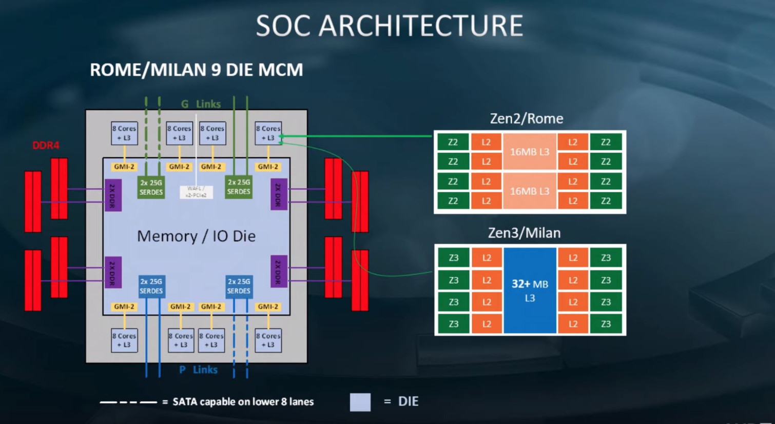
With its next-generation "Zen 3" CPU microarchitecture designed for the 7 nm EUV silicon fabrication process, AMD could bid the "Zen" compute complex or CCX farewell, heralding chiplets with monolithic last-level caches (L3 caches) that are shared across all cores on the chiplet. AMD embraced a quad-core compute complex approach to building multi-core processors with "Zen." At the time, the 8-core "Zeppelin" die featured two CCX with four cores, each. With "Zen 2," AMD reduced the CPU chiplet to only containing CPU cores, L3 cache, and an Infinity Fabric interface, talking to an I/O controller die elsewhere on the processor package. This reduces the economic or technical utility in retaining the CCX topology, which limits the amount of L3 cache individual cores can access.

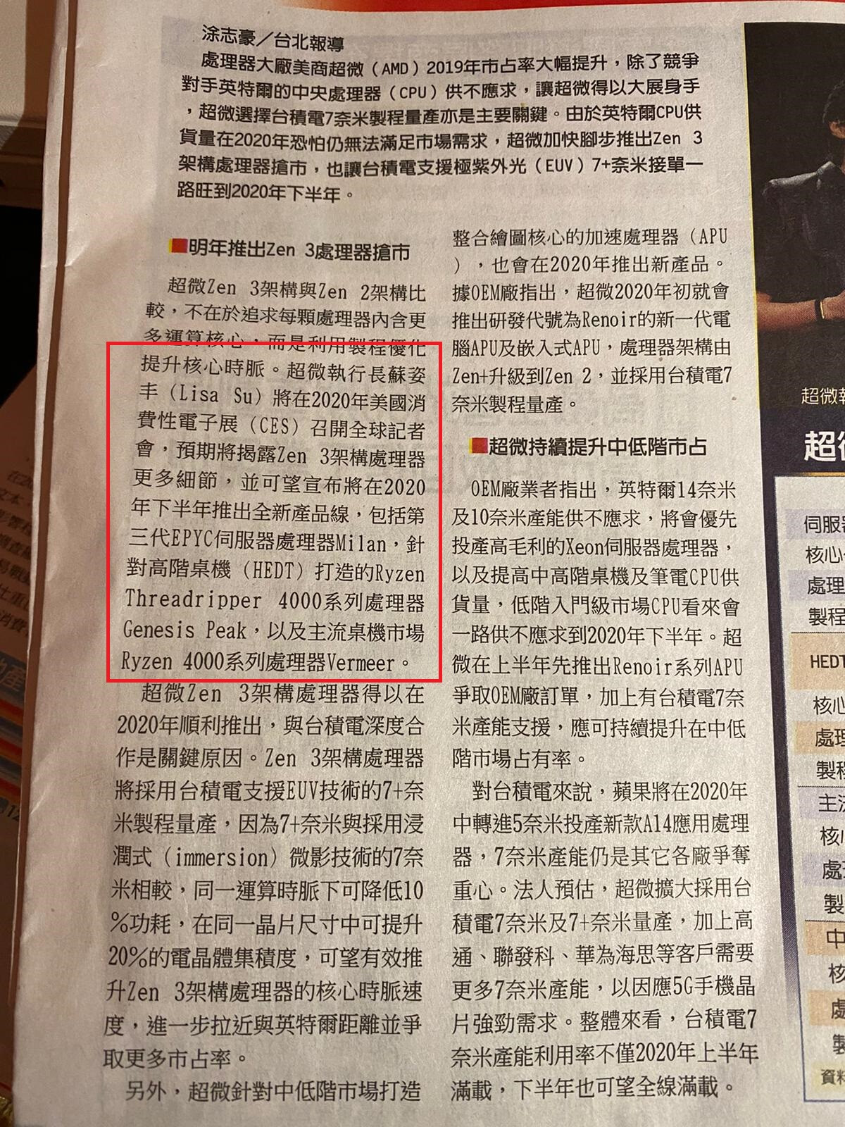
This and more juicy details about "Zen 3" were put out by a leaked (later deleted) technical presentation by company CTO Mark Papermaster. On the EPYC side of things, AMD's design efforts will be spearheaded by the "Milan" multi-chip module, featuring up to 64 cores spread across eight 8-core chiplets. Papermaster talked about how the individual chiplets will feature "unified" 32 MB of last-level cache, which means a deprecation of the CCX topology. He also detailed an updated SMT implementation that doubles the number of logical processors per physical core. The I/O interface of "Milan" will retain PCI-Express gen 4.0 and eight-channel DDR4 memory interface.
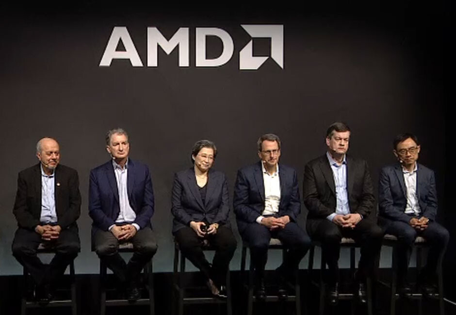
Return to Keyword Browsing
May 31st, 2024 07:20 EDT change timezone

New Forum Posts

Popular Reviews

Controversial News Posts