News Posts matching #Navi 31

Return to Keyword Browsing

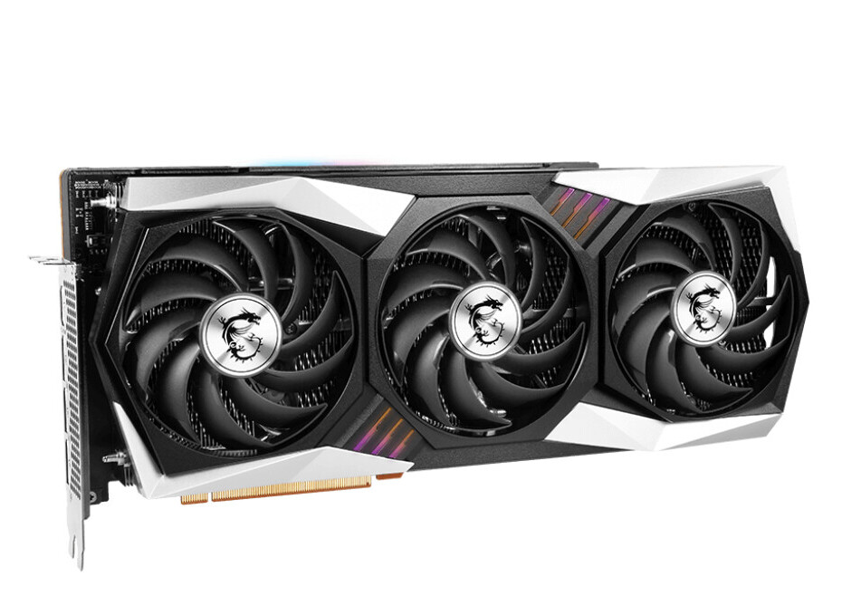
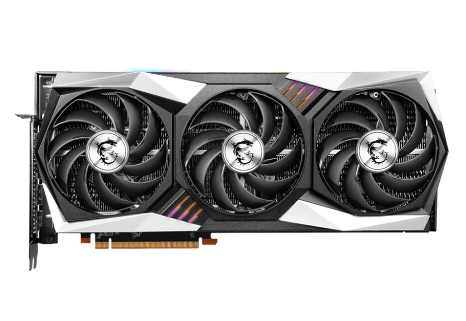
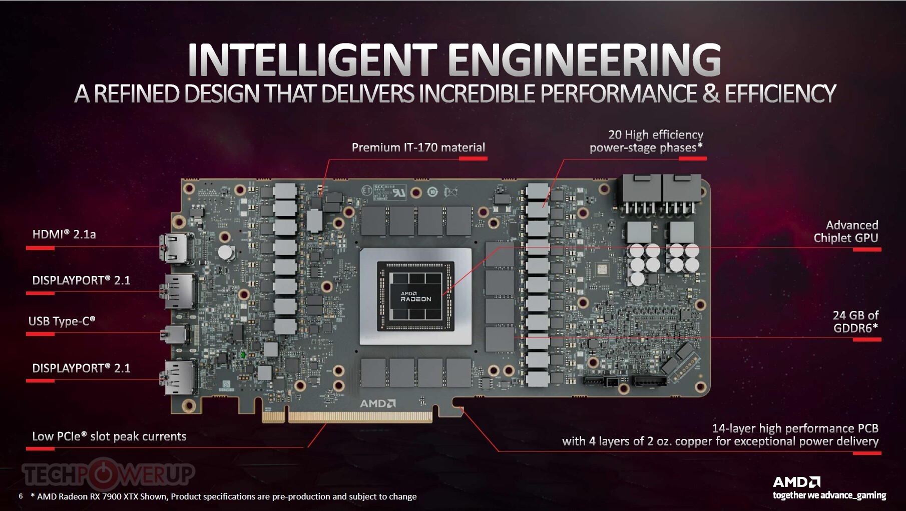
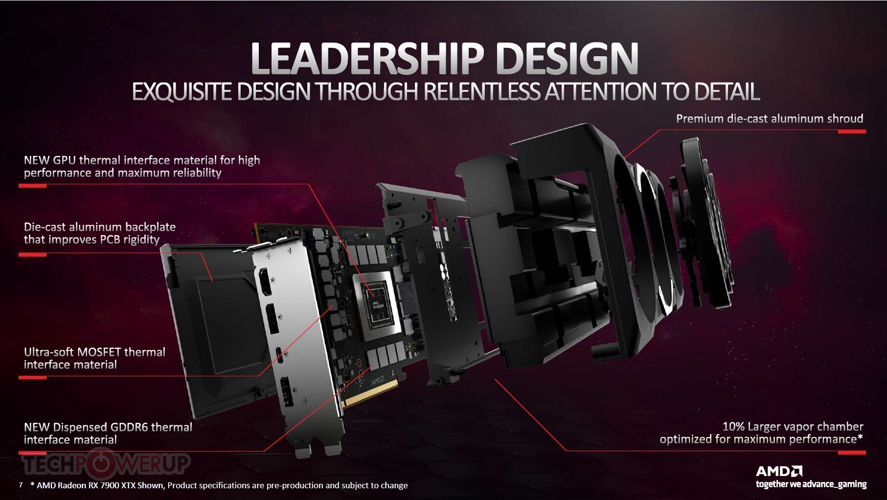
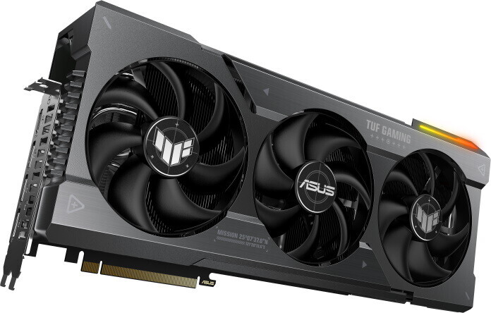
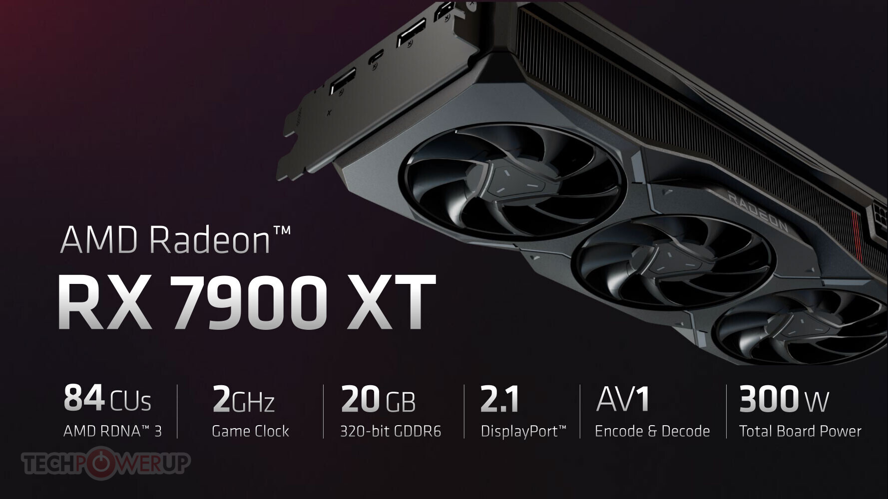
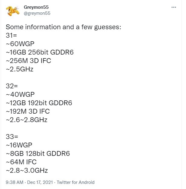
Powercolor RX 7900 XTX Hellhound White Edition GPU Incoming

Powercolor has teased an upcoming reveal, set to happen on April 11, for a White Hellhound Edition of what appears to be (hash-tagged) an AMD Radeon RX 7900 XTX graphics card. A single image of the soon to be revealed model was uploaded to various Powercolor social media sites today. The Specral White colorway is likely applied to the PCB, backplate, fans, bracket and shroud. Powercolor has a consistent history of releasing all-white Hellhound edition cards - quite the rare aesthetic in this market segment.

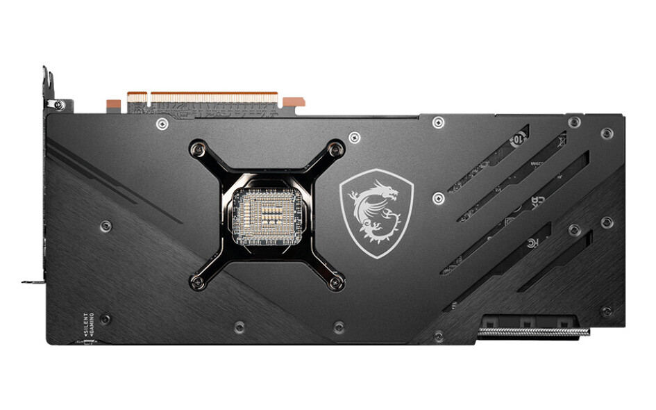
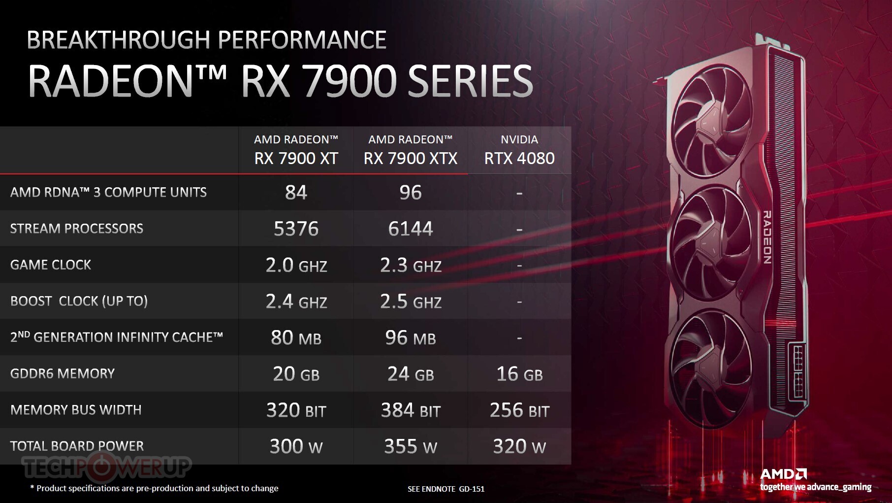
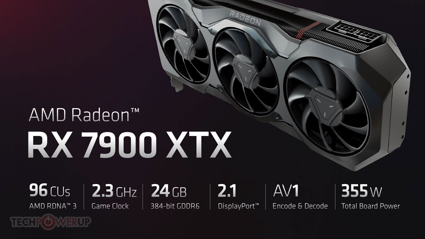
The current black version of the Hellhound AMD Radeon RX 7900 XTX was released last December. The upcoming Specral White iteration seems to share the same LED switching system and twin 8-pin PCIe power inputs - as seen in the teaser image. By and large the specification and feature sets are anticipated to be identical between each model.

MSI Radeon RX 7900 XTX Gaming Trio Classic Listed at $1100

MSI Radeon RX 7900 XTX Gaming Trio Classic, the company's first Radeon 7000 series RDNA3 graphics card, is finally listed online. American retailer Newegg put it up for sale at $1,100, a $100 premium over the $1000 AMD baseline price for the RX 7900 XTX. This is a "sold and shipped by Newegg" listing. MSI showed this card off last month, at the 2023 International CES. It pairs a custom-design PCB with a previous-generation Tri Frozr 2.0 cooling solution—the same one it used with its RX 6950 XT Gaming series. The PCB, however, is an MSI in-house design, with a meaty VRM that draws power from three 8-pin PCIe power connectors, and should hence feature a higher power-limit than the reference-design board, which has been known to scoop out a far greater overclocking headroom on other cards with a similar power setup (such as the ASUS TUF Gaming RX 7900 XTX).

The MSI RX 7900 XTX Gaming Trio Classic comes with clock speeds of 2.30 GHz game, and 2.50 GHz boost, which surprisingly are AMD's reference clocks. Perhaps MSI is saving factory-overclocks for the RX 7900 XTX Gaming X Trio Classic, which it will price even higher. Maxing out the 5 nm "Navi 31" GPU, the RX 7900 XTX offers 6,144 stream processors across 96 RDNA3 compute units, with 96 Ray Accelerators, 384 TMUs, 192 ROPs, and a 384-bit wide GDDR6 memory interface, running 24 GB of memory at 20 Gbps (960 GB/s memory bandwidth).

AMD "Navi 31" Memory Cache Die Has Preparation for 3D Vertical Cache?

AMD possibly has a straightforward path to increasing the performance of the "Navi 31" RDNA3 GPU to power future high-end SKUs, according to semiconductor engineer Tom Wassick. The GPU's main SIMD machinery is located in the Graphics Compute Die (GCD) built on the 5 nm EUV foundry process, surrounded by six Memory Cache Dies (MCDs) built on 6 nm, which each contain GDDR6 memory controllers, and a 16 MB segment of the GPU's 96 MB Infinity Cache memory.

In microscopic observations, Wassick noticed structures on the MCD which he thinks look like an array of through-silicon vias (TSVs), of the kind used in "Zen 3" and "Zen 4" CCDs, to wire out stacked 3D Vertical Cache memory on the L3D (L3 cache die). If the theory holds up, it could be possible for AMD to increase the L3 cache segment size per MCD from 16 MB, and the GPU's overall Infinity Cache memory size. With its RDNA2 graphics architecture (RX 6000 series), AMD significantly enlarged on-die caches on its GPUs, particularly the last-level L3 cache, even giving them the special branding of "Infinity Cache," claiming that they had a big impact in lubricating the memory sub-system, letting GPUs with 256-bit memory buses compete with NVIDIA GPUs with wider 320-bit to 384-bit interfaces.

AMD Confirms Radeon RX 7900 Series Clocks, Direct Competition with RTX 4080

AMD in its technical presentation confirmed the reference clock speeds of the Radeon RX 7900 XTX and RX 7900 XT RDNA3 graphics cards. The company also made its first reference to a GeForce RTX 40-series "Ada" product, the RTX 4080 (16 GB), which is going to launch later today. The RX 7900 XTX maxes out the "Navi 31" silicon, featuring all 96 RDNA3 compute units or 6,144 stream processors; while the RX 7900 XT is configured with 84 compute units, or 5,376 stream processors. The two cards also differ with memory configuration. While the RX 7900 XTX gets 24 GB of 20 Gbps GDDR6 across a 384-bit memory interface (960 GB/s); the RX 7900 XT gets 20 GB of 20 Gbps GDDR6 across 320-bit (800 GB/s).

The RX 7900 XTX comes with a Game Clocks frequency of 2300 MHz, and 2500 MHz boost clocks, whereas the RX 7900 XT comes with 2000 MHz Game Clocks, and 2400 MHz boost clocks. The Game Clocks frequency is more relevant between the two. AMD achieves 20 GB memory on the RX 7900 XT by using ten 16 Gbit GDDR6 memory chips across a 320-bit wide memory bus created by disabling one of the six 64-bit MCDs, which also subtracts 16 MB from the GPU's 96 MB Infinity Cache memory, leaving the RX 7900 XT with 80 MB of it. The slide describing the specs of the two cards compares them to the GeForce RTX 4080, which is what the two could compete more against, especially given their pricing. The RX 7900 XTX is 16% cheaper than the RTX 4080, and the RX 7900 XT is 25% cheaper.

AMD Radeon RX 7900 XTX Reference Design PCB and Cooler Detailed

AMD Radeon RX 7900 XTX reference-design isn't a first-party product with limited availability like the NVIDIA Founders Edition; but rather a classic reference-design that's sold by AMD's add-in board partners under their marquee (without sticking their own labels on the product). AMD and its partners internally refer to reference-design cards as "MBA cards" (made by AMD cards). The company gave us a technical overview of the reference-design PCB. As with every reference AMD PCB for the past several generations, the RX 7900 XTX PCB has a premium selection of components. The card uses an expensive 14-layer PCB with 4 additional layers of 2-oz copper. 14-layer PCBs are typically used with enterprise-grade products, and graphics cards typically tend to have PCB layer counts of around 10. The PCB also uses ITEQ IT-170GRA epoxy and laminate materials, which enable a glass transition temperature (Tg) of 175 °C (no, the GPU won't get anywhere near as hot).

The reference-design RX 7900 XTX PCB draws power from two 8-pin PCIe power connectors. With the typical board power of the RX 7900 XTX rated at 355 W, this falls inside the 375 total power-draw capability when you add up the 150 W input from the two connectors, and 75 W from the PCIe slot. AMD worked to minimize power-draw spikes at least from the PCIe slot. Excursions, if any, should be localized to the 8-pin power connectors. The card features 20-phase VRM solution, using "high efficiency" DrMOS power-stage phases (could be very high current). The "Navi 31" GPU is surrounded by 12 GDDR6 memory chips given the GPU's 384-bit memory interface. Two of these memory pads could end up unused on the RX 7900 XT, which has a 320-bit memory interface. Display outputs of the RX 7900 series include two standard-size DisplayPort 2.1, one USB type-C with DisplayPort passthrough; and one HDMI 2.1a.

AMD Explains the Economics Behind Chiplets for GPUs

AMD, in its technical presentation for the new Radeon RX 7900 series "Navi 31" GPU, gave us an elaborate explanation on why it had to take the chiplets route for high-end GPUs, devices that are far more complex than CPUs. The company also enlightened us on what sets chiplet-based packages apart from classic multi-chip modules (MCMs). An MCM is a package that consists of multiple independent devices sharing a fiberglass substrate.

An example of an MCM would be a mobile Intel Core processor, in which the CPU die and the PCH die share a substrate. Here, the CPU and the PCH are independent pieces of silicon that can otherwise exist on their own packages (as they do on the desktop platform), but have been paired together on a single substrate to minimize PCB footprint, which is precious on a mobile platform. A chiplet-based device is one where a substrate is made up of multiple dies that cannot otherwise independently exist on their own packages without an impact on inter-die bandwidth or latency. They are essentially what should have been components on a monolithic die, but disintegrated into separate dies built on different semiconductor foundry nodes, with a purely cost-driven motive.

AMD RDNA3 Navi 31 GPU Block Diagram Leaked, Confirmed to be PCIe Gen 4

An alleged leaked company slide details AMD's upcoming 5 nm "Navi 31" GPU powering the next-generation Radeon RX 7900 XTX and RX 7900 XT graphics cards. The slide details the "Navi 31" MCM, with its central graphics compute die (GCD) chiplet that's built on the 5 nm EUV silicon fabrication process, surrounded by six memory cache dies (MCDs), each built on the 6 nm process. The GCD interfaces with the system over a PCI-Express 4.0 x16 host interface. It features the latest-generation multimedia engine with dual-stream encoders; and the new Radiance display engine with DisplayPort 2.1 and HDMI 2.1a support. Custom interconnects tie it with the six MCDs.

Each MCD has 16 MB of Infinity Cache (L3 cache); and a 64-bit GDDR6 memory interface (two 32-bit GDDR6 paths). Six of these add up to the GPU's 384-bit GDDR6 memory interface. In the scheme of things, the GPU has a contiguous and monolithic 384-bit wide memory bus, because every modern GPU uses multiple on-die memory controllers to achieve a wide memory bus. "Navi 31" hence has a total Infinity Cache size of 96 MB—which may be less in comparison to the 128 MB on "Navi 21," but AMD has shored up cache sizes across the GPU. The L0 caches on the compute units is now increased numerically by 240%. The L1 caches by 300%, and the L2 cache shared among the shader engines, by 50%. The RX 7900 XTX is confirmed to use 20 Gbps GDDR6 memory in this slide, for 960 GB/s of memory bandwidth.

AMD's Navi 31 Might Clock to 3 GHz, Partner Cards Will be Able to Overclock

Based on details from a PCWorld livestream following AMD's launch of the Radeon RX 7000-series, it was revealed that AMD has designed the Navi 31 GPU to be able to scale as high as 3 GHz. In other words, it appears that AMD has power limited its cards, at least for the SKUs that the company has announced so far. This could be for many reasons, but most likely to try to find a balance between power and performance. The details of the 3 GHz scaling did however not come from AMD directly, but rather from Jarred Walton over at Tom's Hardware. That said, the information was apparently shared with the media by AMD at the event.

In the livestream, it was also confirmed that partner cards will be able to overclock, so expect to see some factory overclocked cards, with higher power draw. This could be why, in part, that ASUS went with a much larger cooler on its TUF Gaming Radeon RX 7900-series cards. As ASUS didn't reveal any clock speeds or TDPs of its two cards, we don't really know what to expect, but we'd be surprised if these cards weren't factory overclocked to some degree when they launch in December.

AMD Announces the $999 Radeon RX 7900 XTX and $899 RX 7900 XT, 5nm RDNA3, DisplayPort 2.1, FSR 3.0 FluidMotion

AMD today announced the Radeon RX 7900 XTX and Radeon RX 7900 XT gaming graphics cards debuting its next-generation RDNA3 graphics architecture. The two new cards come at $999 and $899—basically targeting the $1000 high-end premium price point.
Both cards will be available on December 13th, not only the AMD reference design, which is sold through AMD.com, but also custom-design variants from the many board partners on the same day. AIBs are expected to announce their products in the coming weeks.

The RX 7900 XTX is priced at USD $999, and the RX 7900 XT is $899, which is a surprisingly small difference of only $100, for a performance difference that will certainly be larger, probably in the 20% range. Both Radeon RX 7900 XTX and RX 7900 XT are using the PCI-Express 4.0 interface, Gen 5 is not supported with this generation. The RX 7900 XTX has a typical board power of 355 W, or about 95 W less than that of the GeForce RTX 4090. The reference-design RX 7900 XTX uses conventional 8-pin PCIe power connectors, as would custom-design cards, when they come out. AMD's board partners will create units with three 8-pin power connectors, for higher out of the box performance and better OC potential. The decision to not use the 16-pin power connector that NVIDIA uses was made "well over a year ago", mostly because of cost, complexity and the fact that these Radeons don't require that much power anyway.

AMD Navi 31 RDNA3 GPU Pictured

Here's the first picture of the "Navi 31" GPU at the heart of AMD's fastest next-generation graphics cards. Based on the RDNA3 graphics architecture, this will mark an ambitious attempt by AMD to build the first multi-chip module (MCM) client GPU featuring more than one logic die. MCM GPUs aren't new in the enterprise space with Intel's "Ponte Vecchio," but this would be the first such GPU meant for hardcore gaming graphics products. AMD had made MCM GPUs in the past, but those have been packages with just one logic die, surrounded by memory stacks. "Navi 31" is an MCM of as many as eight logic dies, and no memory stacks (no, those aren't HBM stacks in the picture below).

It's rumored that "Navi 31" features one or two SIMD chiplets dubbed GCDs, featuring the GPU's main number crunching machinery, the RDNA3 compute units. These chiplets are likely built on the most advanced silicon fabrication node, likely TSMC 5 nm EUV, but we'll see. The GDDR6 memory controllers handling the chip's 384-bit wide GDDR6 memory interface, will be located on separate chiplets built on a slightly older node, such as TSMC 6 nm. This is not multi-GPU-a-stick, because both SIMD chiplets have uniform access to the entire 384-bit wide memory bus (which is not 2x 192-bit but 1x 384-bit), besides the other ancillaries. The "Navi 31" MCM are expected to be surrounded by JEDEC-standard 20 Gbps GDDR6 memory chips.

AMD Radeon RX 7000 RDNA3 To Launch Early December

AMD's next-generation Radeon RX 7000-series graphics cards based on the RDNA3 graphics architecture, are expected to launch in early-December 2022, according to greymon55, a reliable source with AMD leaks. The cards will be unveiled at a media event to be held on November 3, 2022, with market availability following a month after (between 1st to 5th December). The company is expected to take a top-down product-stack release cycle similar to that of NVIDIA, with the release of two of its top SKUs, the Radeon RX 7900 XTX and the RX 7900 XT. Both these cards are based on the 5 nm Navi 31 MCM GPU. This will be AMD's first client-graphics MCM GPU with more than one logic die. The company has a decade of experience with MCMs, but past generations have been one logic die surrounded with on-package HBM. Navi 31 has on-package logic chiplets, but discrete GDDR6 memory, like most other GPUs in the market today. It's rumored that the company is targeting a 100% performance uplift over the previous-generation, which means team-red is on the prowl to compete with NVIDIA's fastest SKUs, including the RTX 4090 and upcoming RTX 4080.

AMD RDNA3 Radeon RX 7000 Flagship GPU PCB Sketched

Here's the very first sketch of an AMD RDNA3 Radeon RX 7000-series flagship graphics card with the "Navi 31" chip in the middle. This will be AMD's first chiplet-based GPU built on a philosophy similar to that of the Ryzen desktop and EPYC server processors. The main number crunching machinery that benefits the most from the latest foundry process, will be built on 5 nm logic chiplets (up to two of these on the "Navi 31," one of these on the "Navi 32"), while the components that don't really benefit from the latest process, such as the memory controllers, display/media accelerators, etc., will be disintegrated into chiplets built on a slightly older node, such as 6 nm. This way AMD gets to maximize its 5 nm allocation at TSMC, which it has to share among not just the logic tiles of RDNA3 GPUs, but also its "Zen 4" processors.

The top-dog "Navi 31" silicon is expected to feature a 384-bit wide GDDR6 memory interface, which is why you see 12 memory chips surrounding the GPU package. AMD is expected to deploy fast 19-21 Gbps class GDDR6 memory chips, as well as double-down on the Infinity Cache technology. The package looks like a GPU die surrounded by HBM stacks, but those are actually the memory/display chiplets. If this PCB is from an AMD reference design, it could be the biggest hint that AMD isn't switching over to the 12+4 pin ATX 12HPWR connector just yet, and could stick with three 8-pin PCIe connectors for power, just like the current RX 6950 XT. USB-C with DisplayPort passthrough could prominently feature with RDNA3 graphics cards, besides standard DisplayPort and HDMI connectors.

AMD "Navi 31" Rumored to Feature 384-bit GDDR6 Memory Interface

AMD has historically thrown brute memory bus width at solving memory-management problems in its graphics architectures, but the Infinity Cache technology launched with RDNA2 proved to be a game changer, as GPUs with narrow 256-bit memory interfaces could compete with NVIDIA's offerings that have 384-bit wide memory interfaces and faster GDDR6X memory types. It looks like the competition between NVIDIA "Ada" and AMD RDNA3 graphics architectures is about to heat up, as rumors are emerging of AMD giving its biggest next-gen ASIC, the "Navi 31," a 384-bit wide memory interface.

This 50 percent increase in memory bus width, runs in concert with two associated rumors—one, that the company will use faster 20 Gbps GDDR6 memory chips; and two, that AMD may increase the size of the on-die Infinity Cache memory. Samsung is already mass-producing 20 Gbps and 24 Gbps GDDR6 memory chips. These are regular GDDR6 memory chips with JEDEC-standard signaling, and not GDDR6X, an exclusive memory type innovated by NVIDIA and Micron Technology, which leverages PAM4 signaling to increase data-rates. A theoretical "Navi 31" with 20 Gbps GDDR6 memory speeds would enjoy 960 GB/s of memory bandwidth, a massive 87.5 percent bandwidth increase over the RX 6900 XT. The on-die Infinity Cache operates at speeds measured in several TB/s. The increased bus width could also signal an increase in memory sizes, with the RX 6950 XT successor featuring at least 24 GB of memory.

New Specs of AMD RDNA3 GPUs Emerge

A new list of specifications of AMD's next-generation "Navi 3x" GPUs based on the RDNA3 graphics architecture emerged, with lower CU counts than previously reported. It turns out that the large "Navi 31" GPU comes with 12,288 stream processors across 48 WGP (workgroup processors), 12 SA (shader arrays), and 6 SE (shader engines). This still amounts to a 140% increase in stream processors over the Navi 21. This chip will power SKUs that succeed the Radeon RX 6800-series and RX 6900-series.

The second largest silicon from the series is the Navi 32, with two-thirds the number-crunching machinery of the Navi 31. That's 8,192 stream processors across 32 WGPs, 8 SAs, and 4 SEs. The Navi 32 silicon powers successors of the RX 6700-series. The third largest chip is the Navi 33, with half the muscle of the Navi 32, and one-third that of the Navi 31. This means 4,096 stream processors spread across 16 WGP, 4 SA, and 2 SE. There's no word on other specs such as memory bus width, but we've heard rumors of AMD doubling down on the Infinity Cache memory technology, by giving these chips even larger on-die caches. RDNA3 is also expected to improve ray tracing performance, as more of the ray tracing pipeline is handled by fixed-function hardware.

NVIDIA AD102 and AMD Navi 31 in a Race to Reach 100 TFLOPs FP32 First

A technological race is brewing between NVIDIA and AMD over which brand's GPU reaches the 100 TFLOP/s peak FP32 throughput mark first. AMD's TeraScale graphics architecture and the "RV770" silicon, were the first to hit the 1 TFLOP/s mark, way back in 2008. It would take 14 years for this figure to reach 100 TFLOP/s for flagship GPUs. NVIDIA's next generation big GPU based on the "Ada Lovelace," the AD102, is the green team's contender for the 100 TFLOP/s mark, according to kopite7kimi. To achieve this, all 144 streaming multiprocessors (SM) or 18,432 CUDA cores, of the AD102 will have to be enabled.

From the red team, the biggest GPU based on the next-generation RDNA3 graphics architecture, "Navi 31," could offer peak FP32 throughput of 92 TFLOP/s according to greymon55, which gives AMD the freedom to create special SKUs running at high engine clocks, just to reach the 100 TFLOP/s mark. The Navi 31 silicon is expected to triple the compute unit count over its predecessor, resulting in 15,360 stream processors. Both the AD102 and Navi 31 are expected to be built on the same TSMC N5 (5 nm EUV) node, and product launches for both are expected by year-end.

"Navi 31" RDNA3 Sees AMD Double Down on Chiplets: As Many as 7

Way back in January 2021, we heard a spectacular rumor about "Navi 31," the next-generation big GPU by AMD, being the company's first logic-MCM GPU (a GPU with more than one logic die). The company has a legacy of MCM GPUs, but those have been a single logic die surrounded by memory stacks. The RDNA3 graphics architecture that the "Navi 31" is based on, sees AMD fragment the logic die into smaller chiplets, with the goal of ensuring that only those specific components that benefit from the TSMC N5 node (6 nm), such as the number crunching machinery, are built on the node, while ancillary components, such as memory controllers, display controllers, or even media accelerators, are confined to chiplets built on an older node, such as the TSMC N6 (6 nm). AMD had taken this approach with its EPYC and Ryzen processors, where the chiplets with the CPU cores got the better node, and the other logic components got an older one.

Greymon55 predicts an interesting division of labor on the "Navi 31" MCM. Apparently, the number-crunching machinery is spread across two GCD (Graphics Complex Dies?). These dies pack the Shader Engines with their RDNA3 compute units (CU), Command Processor, Geometry Processor, Asynchronous Compute Engines (ACEs), Rendering Backends, etc. These are things that can benefit from the advanced 5 nm node, enabling AMD to the CUs at higher engine clocks. There's also sound logic behind building a big GPU with two such GCDs instead of a single large GCD, as smaller GPUs can be made with a single such GCD (exactly why we have two 8-core chiplets making up a 16-core Ryzen processors, and the one of these being used to create 8-core and 6-core SKUs). The smaller GCD would result in better yields per wafer, and minimize the need for separate wafer orders for a larger die (such as in the case of the Navi 21).

AMD Radeon "Navi 3x" Could See 50% Increase in Shaders, Double the Cache Memory

AMD's next generation Radeon "Navi 3x" line of GPUs could see a 50% increase in shaders and a doubling Infinity Cache memory size, according to some educated-guesswork and intelligence by Greymon55, a reliable source with GPU leaks. The Navi 31, Navi 32, and Navi 33 chips are expected to debut the new RDNA3 graphics architecture, and succeed the 6 nm optical-shrinks of existing Navi 2x chips that AMD is rumored to be working on.

The top Navi 31 part allegedly features 60 workgroup processors (WGPs), or 120 compute units. Assuming an RDNA3 CU still holds 64 stream processors, you're looking at 7,680 stream processors, a 50% increase over Navi 21. The Navi 32 silicon features 40 WGPs, and exactly the same number of shaders as the current Navi 21, at 5,120. The smallest of the three, the Navi 33, packs 16 WGPs, or 2,048 shaders. There is a generational doubling in cache memory, with 256 MB on the Navi 31, 192 MB on the Navi 32, and 64 MB on the Navi 33. Interestingly, the memory sizes and bus widths are unchanged, but AMD could leverage faster GDDR6 memory types. 2022 will see the likes of Samsung ship GDDR6 chips with data-rates as high as 24 Gbps.

AMD Radeon RX 7000 Series to Include 6nm Optical-Shrinks of RDNA2

AMD's upcoming Radeon RX 7000 series could include GPUs from both the RDNA3 and RDNA2 graphics architectures, according to reliable sources on social media. This theory holds that the company could introduce new 5 nm GPUs based on the new RDNA3 architecture for the higher end, namely the Navi 31 and Navi 32; while giving the current-gen RDNA2 architecture a new lease of life in the lower segments. This isn't, however, a simple rebrand.

Apparently, some existing Navi 2x series chips will receive an optical shrink to the 6 nm node, in a bid to improve their performance/Watt. Some of the performance/Watt improvement could be used to increase engine clocks. These include the Navi 22, with its 40 RDNA2 compute units and 192-bit GDDR6 memory bus; and the Navi 23, with its 32 RDNA2 compute units and 128-bit GDDR6 memory bus. The updated Navi 22 will power the SKU that succeeds the current RX 6600 XT, while the updated Navi 23 works the lower-mainstream SKU RX x500-class.

Next-Gen AMD Radeon RDNA3 Flagship To Feature 15,360 Stream Processors?

AMD's next generation RDNA3 graphics architecture generation could see a near-quadrupling in raw SIMD muscle over the current RDNA2, according to a spectacular rumor. Apparently, the company will deploy as many as 15,360 stream processors (quadruple that of a Radeon RX 6800), and spread across 60 WGPs (Workgroup Processors), and do away with the compute unit. This is possibly because the RDNA3 compute unit won't be as independent as the ones on the original RDNA or even RDNA2, which begins to see groups of two CUs share common resources.

Another set of rumors suggest that AMD won't play NVIDIA's game of designing GPUs with wide memory bus widths, and instead build on its Infinity Cache technology, by increasing the on-die cache size and bandwidth, while retaining "affordable" discrete memory bus widths, such as 256-bit. As for the chip itself, it's rumored that the top RDNA3 part, the so-called "Navi 31," could feature a multi-chip module design (at least two logic dies), each with 30 WGPs. Each of the two is expected to be built on a next-gen silicon fabrication node that's either TSMC N5 (5 nm), or a special 6 nm node TSMC is designing for AMD. Much like the next-generation "Lovelace" architecture by NVIDIA, AMD's RDNA3 could see the light of the day only in 2022.

AMD is Allegedly Preparing Navi 31 GPU with Dual 80 CU Chiplet Design

AMD is about to enter the world of chiplets with its upcoming GPUs, just like it has been doing so with the Zen generation of processors. Having launched a Radeon RX 6000 series lineup based on Navi 21 and Navi 22, the company is seemingly not stopping there. To remain competitive, it needs to be in the constant process of innovation and development, which is reportedly true once again. According to the current rumors, AMD is working on an RDNA 3 GPU design based on chiplets. The chiplet design is supposed to feature two 80 Compute Unit (CU) dies, just like the ones found inside the Radeon RX 6900 XT graphics card.

Having two 80 CU dies would bring the total core number to exactly 10240 cores (two times 5120 cores on Navi 21 die). Combined with the RDNA 3 architecture, which brings better perf-per-watt compared to the last generation uArch, Navi 31 GPU is going to be a compute monster. It isn't exactly clear whatever we are supposed to get this graphics card, however, it may be coming at the end of this year or the beginning of the following year 2022.

Apple MacOS "Big Sur" Beta Driver Code Points to AMD "Navi 31" GPU

AMD's "Navi 20-series" GPUs implementing the RDNA2 graphics architecture are barely close to launch (September 2020 unveiling expected); and there's already talk of the "Navi 30-series." When digging through the driver code for AMD Radeon graphics that ships with Apple's MacOS "Big Sur" developer beta 1, Hardware Leaks (_rogame) uncovered pointers to an AMD "navi31" GPU. This could be the very first indication that AMD will codename successors of the RDNA2-based "Navi 2#" GPUs, such as the "Navi 21," under the "Navi 3#" series. It remains to be seen if these chips implement the RDNA3 graphics architecture, or are a refresh of RDNA2-based chips on a newer process.
Return to Keyword Browsing
May 21st, 2024 15:16 EDT change timezone

New Forum Posts

Popular Reviews

Controversial News Posts