Wednesday, August 18th 2021

AMD Radeon RX 7000 Series to Include 6nm Optical-Shrinks of RDNA2

AMD's upcoming Radeon RX 7000 series could include GPUs from both the RDNA3 and RDNA2 graphics architectures, according to reliable sources on social media. This theory holds that the company could introduce new 5 nm GPUs based on the new RDNA3 architecture for the higher end, namely the Navi 31 and Navi 32; while giving the current-gen RDNA2 architecture a new lease of life in the lower segments. This isn't, however, a simple rebrand.

Apparently, some existing Navi 2x series chips will receive an optical shrink to the 6 nm node, in a bid to improve their performance/Watt. Some of the performance/Watt improvement could be used to increase engine clocks. These include the Navi 22, with its 40 RDNA2 compute units and 192-bit GDDR6 memory bus; and the Navi 23, with its 32 RDNA2 compute units and 128-bit GDDR6 memory bus. The updated Navi 22 will power the SKU that succeeds the current RX 6600 XT, while the updated Navi 23 works the lower-mainstream SKU RX x500-class.
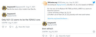
It's also conceivable that AMD uses the opportunity to update the display and media-acceleration components of the chips, as it's been doing with the latest applications of "Vega," such as the iGPU inside Ryzen 5000G processors. RDNA3, meanwhile, will likely power the two largest chips, the 5 nm "Navi 31" and the "Navi 32," which will be at the hearts of SKUs that succeed the RX 6900/6800 series, and the RX 6700 series.
Sources: Greymon55 (Twitter), VideoCardz
Add your own comment

34 Comments on AMD Radeon RX 7000 Series to Include 6nm Optical-Shrinks of RDNA2

#1
HenrySomeone
"This isn't, however, a simple rebrand."
Coming from the kings of rebrand....yeah we'll believe it when we see it
Posted on Reply
#2
dj-electric
Gee,
TSMC's 6nm node seems cool.

I wonder what other GPUs could be made there.
If only i could have my crystal ball... or beaker or cauldron... or potions or mystical components to make a special way to see things...
Posted on Reply
#3
Cheese_On_tsaot
HenrySomeone"This isn't, however, a simple rebrand."
Coming from the kings of rebrand....yeah we'll believe it when we see it
To be fair, that GTS 250 was just an 8800 GT.
Posted on Reply
#4
windwhirl
HenrySomeone"This isn't, however, a simple rebrand."
Coming from the kings of rebrand....yeah we'll believe it when we see it
You say that as if Nvidia didn't do the same.
Posted on Reply
#5
londiste
N6 should be pretty much the same as N7+ when it comes to density. No real word on any other improvements. The main technical difference should be one more EUV layer.
This may not exactly be a significant die shrink.
Posted on Reply
#6
Franzen4Real
londisteN6 should be pretty much the same as N7+ when it comes to density. No real word on any other improvements. The main technical difference should be one more EUV layer.
This may not exactly be a significant die shrink.
Perhaps the end result being something similar to the RX590 12nm refresh?

edit-- meant that in reference to the RDNA2 cards..
Posted on Reply
#7
BorisDG
Was kinda expected, since new revision of PS5 using 6nm chip was rumored for a while.
Posted on Reply
#8
londiste
Franzen4RealPerhaps the end result being something similar to the RX590 12nm refresh?
That sounds likely. Minor optimizations, small efficiency boost but nothing major. The GPUs are pretty good so they should fine enough with that.
Posted on Reply
#9
Darmok N Jalad
HenrySomeone"This isn't, however, a simple rebrand."
Coming from the kings of rebrand....yeah we'll believe it when we see it
Cheese_On_tsaotTo be fair, that GTS 250 was just an 8800 GT.
windwhirlYou say that as if Nvidia didn't do the same.
While all have been guilty, I think all the Kaby Lake refreshes may hold the crown.
Posted on Reply
#10
HisDivineOrder
I love AMD's strategy. The high end is currently where any value is, if you assume MSRP's aren't a fiction (which they are). The lower end? Everyone is saying the latest card has no value because of it's 1080p-focused, $380 pricing.

So AMD's response for future products?

Have moar of the same at the low end, improve the high end once again. You can't make this stuff up. All they need to do is increase prices and they'll doing their very best nvidia cosplay.
Posted on Reply
#11
Tigerfox
Cheese_On_tsaotTo be fair, that GTS 250 was just an 8800 GT.
No, it wasn't, an it doesn't become more true if people repeat this lie.

If anything, it was a rebranded 8800 GTS 512, but even that is not true. 8800 GTS 512 used a fully activated G92, which was a shrink of G80 from 80nm to 65nm with a more modern VP, but 256 instad of 384 Bit SI. With a higher core clock, 8800 GTS 512 was an Update of 8800 GTX and 8800 Ultra, but not quite, since the lower memory bandwith an smaller VRAM were bottlenecks in high resulutions with eyecandy. 8800 GTS used the same PCB as 8800 GT, which had one SU deactivated an lower clockrates, but was much faster than 8800 GTS 640.

9800 GTX wasn't a straight rebrand either, since it got a much bigger, beefier PCB with 2x6-Pin PCIe-Power and a bigger cooler and faster VRAM, but only modestly more core clock (OC potential was much better though). It also had Nvidia HybridPower to turn off the dGPU on a nForce-Board with iGPU.
9800 GTX+ was a shrink to 55nm with much better core clock @stock and by OCing and 1GB VRAM as standard.
250 GTS was not a direct rebrand either, it again had a new, smaller PCB with 1x6-Pin and a cooler looking similar to 8800 GTS 512 (but with a different heatsink) and replaced HybridPower with the ability to reduce clockrates and voltages.

I know that was still dissapointingly small progress in GPU-power between 8800 GTX and GTX 280, but Nvidia always (had to) adjust the prices accordingly, because this was one the most price-competetive phases of GPU-history.
9800GT was a direct rebrand of 8800GT, most SKU were identical, only later they were shrunk to 55nm and more often got 1GB VRAM, too.
Posted on Reply
#12
ZoneDymo
All I care about is prices coming down to a NORMAL FFING LEVEL so I can actually convince myself its ok to buy a freaking videocard jeez.
Posted on Reply
#13
Cheese_On_tsaot
TigerfoxNo, it wasn't, an it doesn't become more true if people repeat this lie.

If anything, it was a rebranded 8800 GTS 512, but even that is not true. 8800 GTS 512 used a fully activated G92, which was a shrink of G80 from 80nm to 65nm with a more modern VP, but 256 instad of 384 Bit SI. With a higher core clock, 8800 GTS 512 was an Update of 8800 GTX and 8800 Ultra, but not quite, since the lower memory bandwith an smaller VRAM were bottlenecks in high resulutions with eyecandy. 8800 GTS used the same PCB as 8800 GT, which had one SU deactivated an lower clockrates, but was much faster than 8800 GTS 640.

9800 GTX wasn't a straight rebrand either, since it got a much bigger, beefier PCB with 2x6-Pin PCIe-Power and a bigger cooler and faster VRAM, but only modestly more core clock (OC potential was much better though). It also had Nvidia HybridPower to turn off the dGPU on a nForce-Board with iGPU.
9800 GTX+ was a shrink to 55nm with much better core clock @stock and by OCing and 1GB VRAM as standard.
250 GTS was not a direct rebrand either, it again had a new, smaller PCB with 1x6-Pin and a cooler looking similar to 8800 GTS 512 (but with a different heatsink) and replaced HybridPower with the ability to reduce clockrates and voltages.

I know that was still dissapointingly small progress in GPU-power between 8800 GTX and GTX 280, but Nvidia always (had to) adjust the prices accordingly, because this was one the most price-competetive phases of GPU-history.
9800GT was a direct rebrand of 8800GT, most SKU were identical, only later they were shrunk to 55nm and more often got 1GB VRAM, too.
The GTS 250 vs barely 15% faster than an 8800 GTX and it is on a smaller process and with better clocks so....

Regardless of being either or, it's end performance is that of a an overclocked 8800 GTX.

I forgot the X at the end.. I used to own the 9800 GTX+

Posted on Reply
#14
kruk
It's a smart move that will surely increase next-gen availability (nVidia will 100% do something similar), but the 5nm GPUs from both camps will probably be pretty expensive ...
Posted on Reply
#15
rutra80
At first I thought it's about part of the chip being optic fibre based :ohwell:
Posted on Reply
#16
Mistral
Would it really be a rebrand, if you were never able to buy them in the first place?

I think it's an OK move.
Posted on Reply
#17
windwhirl
MistralWould it really be a rebrand, if you were never able to buy them in the first place?
Can't argue with that logic lol
Posted on Reply
#18
Vader
dj-electricGee,
TSMC's 6nm node seems cool.

I wonder what other GPUs could be made there.
If only i could have my crystal ball... or beaker or cauldron... or potions or mystical components to make a special way to see things...
What you did there, i have seen it
Posted on Reply
#19
TheinsanegamerN
So once again AMD manages to catch up to nvidia and proceeds to rebrand their lineup. AGAIN.

They did this with the HD 5000->HD6000 series

They did this with the HD 7000 -> R200 series

Now they're doing it with the RX 6000->RX7000 series.

If history is any indication Nvidia is going to come out swinging with RTX 4000 and drive AMD back into being the budget brand....again.
Posted on Reply
#20
Darmok N Jalad
TheinsanegamerNSo once again AMD manages to catch up to nvidia and proceeds to rebrand their lineup. AGAIN.

They did this with the HD 5000->HD6000 series

They did this with the HD 7000 -> R200 series

Now they're doing it with the RX 6000->RX7000 series.

If history is any indication Nvidia is going to come out swinging with RTX 4000 and drive AMD back into being the budget brand....again.
Perhaps it’s more like Ryzen 2000, where there was a similar shrink but also a few additional tweaks added that resulted in a clock speed boost and a minor IPC increase. Those were good things, but merely a stop-gap until Ryzen 3000.

Also, if the current market trends continue, there is no such thing as a budget brand.
Posted on Reply
#21
Fourstaff
Not a terrible idea to put maximum engineering resources to work on the flagship, and fill the remaining product stack with "still good" parts.
Posted on Reply
#22
Minus Infinity
Sounds like a rebrand+. Same architecture, just a bit higher clocks and bit better energy usage. I'm guessing 20% dearer and 10% better performance at 10% less power.
Posted on Reply
#23
watzupken
HenrySomeone"This isn't, however, a simple rebrand."
Coming from the kings of rebrand....yeah we'll believe it when we see it
While TSMC's 6nm is basically an improved 7nm, it is supposed to bring some improvement in terms of efficiency. So I won't say that it is a straight rebrand like they used to where they basically rebrand RX 480 to 580.

In any case, it is not uncommon for lower end cards to get this treatment since they are low in profit margin. Main buyers are less particular about not getting cutting edge performance. At the end of the day, if the card performs faster than its predecessor at the same price range, I think it is still a good upgrade.
Posted on Reply
#24
eidairaman1
The Exiled Airman
Minus InfinitySounds like a rebrand+. Same architecture, just a bit higher clocks and bit better energy usage. I'm guessing 20% dearer and 10% better performance at 10% less power.
The lower cards will be RDNA 2 and upper cards RDNA3.

Ellesmere was rebadged 3x.
Posted on Reply
#25
Punkenjoy
I don't see big deal with rebranding itself, as long as the value is good.

That to be seen.
Posted on Reply
Add your own comment
May 15th, 2024 21:50 EDT change timezone

New Forum Posts

Popular Reviews

Controversial News Posts