News Posts matching #Samsung

Return to Keyword Browsing

DEEPX Announces State-of-the-Art AI Chip Product Lineup

DEEPX, a leading AI semiconductor technology company, aims to drive innovation in the rapidly evolving edge AI landscape with its state-of-the-art, low-power, high-performance AI chip product lineup. With a focus on revolutionizing application areas such as smart cities, surveillance, smart factories, and other industries, DEEPX unveiled its latest AI semiconductor solutions at the 2023 Samsung Foundry Forum (SFF), under the theme of "For AI Everywhere."

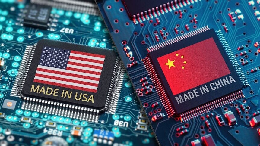
Recognizing the importance of collaboration and technological partnerships, DEEPX leveraged Samsung Electronics' foundry processes, harnessing the power of 5 nm, 14 nm, and 28 nm technologies for its semiconductor chip designs. As a result, the company has developed a suite of four high-performance, energy-efficient AI semiconductor products: DX-L1, DX-L2, DX-M1, and DX-H1. Each product has been specifically engineered to cater to the unique demands of various market segments, from ultra-compact sensors with minimal data processing requirements to AI-intensive applications such as robotics, computer vision, autonomous vehicles, and many others.

Samsung Unveils ViewFinity S9 5K Monitor

Samsung Electronics today announced it is expanding its ViewFinity monitor lineup with the global availability of the 27-inch ViewFinity S9 (S90PC model). The launch of the ViewFinity S9 strengthens Samsung's high-resolution monitor lineup following the introduction of the ViewFinity S8 (S80PB model) in June 2022 which featured an Ultra High Definition (UHD) resolution. The new ViewFinity S9 is optimized with all the tools needed in industries like graphic design and photography and also being named a CES Innovation Award honoree in 2023.

"Our new 5K monitor is designed to deliver the highest performance and best experience for professionals in creative and visual industries," said Hoon Chung, Executive Vice President of the Visual Display Business at Samsung Electronics. "With the ViewFinity lineup, we will provide creatives with top-notch visual experiences, along with the lifelike color clarity and versatile connectivity they need to achieve the best in any project."

Samsung Claims Higher 3 nm Yields than TSMC

Competition between Samsung and TSMC in the 4 nm and 3 nm foundry process markets is about to heat up, with the Korean foundry claiming yields competitive to those of TSMC, according to a report in the Kukmin Ilbo, a Korean daily newspaper. 4 nm is the final silicon fabrication process to use the FinFET technology that powered nodes ranging between 16 nm to 4 nm. Samsung Foundry is claiming 4 nm wafer yields of 75%, against the 80% yields figure put out by TSMC. 4 nm powers several current-generation mobile SoCs, PC processors, and more importantly, the GPUs driving the AI gold-rush.

Things get very interesting with 3 nm, the node that debuts GAA-FET (gates all around FET) technology. Here, Samsung claims to offer higher yields than TSMC, with its 3 nm GAA node clocking 60% yields, against 55% put out by TSMC. Samsung was recently bitten by a scandal where its engineers allegedly falsified yields figures to customers to score orders, which had a cascading effect on the volumes and competitiveness of their customers. We're inclined to think that Samsung has taken lessons and is more careful with the yields figures being reported in the press. Meanwhile, Intel Foundry Services competes with the Intel 3 node, which is physically 7 nm FinFET, but with electrical characteristics comparable to those of 3 nm.

Samsung Starts Mass Production of Automotive UFS 3.1 Memory Solution

Samsung Electronics, a world leader in advanced semiconductor technology, today announced that it has initiated mass production of its new automotive Universal Flash Storage (UFS) 3.1 memory solution optimized for in-vehicle infotainment (IVI) systems. The new solution offers the industry's lowest energy consumption, enabling car manufacturers to provide the best mobility experience for consumers.

The UFS 3.1 lineup will come in 128, 256 and 512-gigabyte (GB) variants to meet different needs of customers. The enhanced lineup allows more efficient battery life management to future automotive applications such as electric or autonomous vehicles. The 256 GB model, for instance, has reduced its energy consumption by about 33% compared to the previous generation product. The 256 GB model also provides a sequential write speed of 700-megabytes-per-second (MB/s) and a sequential read speed of 2,000 MB/s.

Samsung & MediaTek Announce Industry-first 3Tx Antenna Transmission

Samsung Electronics and MediaTek completed the successful testing of 5G Standalone Uplink (UL) 2CC Carrier Aggregation (CA) with C-Band UL MIMO to reach top uplink speeds, marking a groundbreaking achievement in wireless mobile capabilities. This approach used three transmit (3Tx) antennas to improve upload experiences, ushering in an era of enhanced connectivity for consumers worldwide.

The demands on uplink performance are increasing with the rise of live streaming, multi-player gaming and video conferences. Upload speeds determine how fast your device can send data to gaming servers or transmit high-resolution videos to the cloud. As more consumers seek to document and share their experiences with the world in real-time, enhanced uplink experiences provide an opportunity to use the network to improve how they map out their route home, check player stats online and upload videos and selfies to share with friends and followers.

Micron Readying GDDR7 Memory for 2024

Last week Micron Technology CEO, Sanjay Mehrotra, announced during an investors meeting that the company's next generation GPU memory—GDDR7—will be arriving next year: "In graphics, industry analysts continue to expect graphics' TAM compound annual growth rate (CAGR) to outpace the broader market, supported by applications across client and data center. We expect customer inventories to normalize in calendar Q3. We plan to introduce our next-generation G7 product on our industry-leading 1ß node in the first half of calendar year 2024." His proposed launch window seems to align with information gleaned from previous reports—with NVIDIA and AMD lined up to fit GDDR7 SGRAM onto their next-gen mainstream GPUs, although Team Green could be delaying their Ada Lovelace successor into 2025.

Micron already counts these big players as key clients for its current GDDR6 and GDDR6X video memory offerings, but Samsung could be vying for some of that action with its own GDDR7 technology (as announced late last year). Presentation material indicated that Samsung is anticipating data transfer rates in the range of 36 Gbps, with usage of PAM3 signalling. Cadence has also confirmed similar numbers for its (industry first) GDDR7 verification solution, but the different encoding standard will require revising of memory controllers and physical interfaces.

Samsung Launches New Game Portal Online Store

Samsung Electronics today announced that it plans to open Samsung Game Portal, an online store specializing in gaming, on Samsung.com in more than 30 countries around the world, starting with the U.S., the U.K., Germany, France, Italy, Spain and Brazil in late June. The Game Portal is a one-stop online store for gamers designed to significantly increase the convenience of browsing and purchasing products such as smartphones, TVs, gaming monitors and high-performance SSDs. It also provides customers with a variety of gaming-related content in one place, fine-tuned to their preferences and experiences.

In 2021, Accenture, a leading global professional services company, published an illuminating gaming-related study. The study found that half of the gaming population are cross-platform gamers who use more than one device to play, spending an average of 16 hours a week gaming, as well as eight hours a week watching gaming-related video content and six hours a week participating in gaming-related communities. In response to these customer trends, Samsung has designed the Game Portal to provide an impressive variety of content, such as gaming product information, domestic and international expert reviews, product purchase benefits and offers, product utilization ideas that help users enjoy games more and game-related news.

Semiconductor Market Extends Record Decline Into Fifth Quarter

New research from Omdia reveals that the semiconductor market declined in revenue for a fifth straight quarter in the first quarter of 2023. This is the longest recorded period of decline since Omdia began tracking the market in 2002. Revenue in 1Q23 settled at $120.5B, down 9% from 4Q22. The semiconductor market is cyclical, and this prolonged decline follows the upsurge as the market grew to record revenues in each quarter between 4Q20 through 4Q21 following increased demand from the global pandemic.

The memory and MPU market are major areas of the semiconductor market that are contributing to the decline. The MPU market in 1Q23 was $13.1B, just 65% of its size in 1Q22 when it was $20B. The memory market fared worse, with 1Q23 coming in at $19.3B, just 44% of the market in 1Q22 when it was $43.6B. The combined MPU and memory markets declined 19% in 1Q23, dragging the market down to the 9% quarter-over-quarter (QoQ) decline.

Samsung Electronics Unveils Foundry Vision in the AI Era

Samsung Electronics, a world leader in advanced semiconductor technology, today announced its latest foundry technology innovations and business strategy at the 7th annual Samsung Foundry Forum (SFF) 2023. Under the theme "Innovation Beyond Boundaries," this year's forum delved into Samsung Foundry's mission to address customer needs in the artificial intelligence (AI) era through advanced semiconductor technology.

Over 700 guests, from customers and partners of Samsung Foundry, attended this year's event, of which 38 companies hosted their own booths to share the latest technology trends in the foundry industry.

Major CSPs Aggressively Constructing AI Servers and Boosting Demand for AI Chips and HBM, Advanced Packaging Capacity Forecasted to Surge 30~40%

TrendForce reports that explosive growth in generative AI applications like chatbots has spurred significant expansion in AI server development in 2023. Major CSPs including Microsoft, Google, AWS, as well as Chinese enterprises like Baidu and ByteDance, have invested heavily in high-end AI servers to continuously train and optimize their AI models. This reliance on high-end AI servers necessitates the use of high-end AI chips, which in turn will not only drive up demand for HBM during 2023~2024, but is also expected to boost growth in advanced packaging capacity by 30~40% in 2024.

TrendForce highlights that to augment the computational efficiency of AI servers and enhance memory transmission bandwidth, leading AI chip makers such as Nvidia, AMD, and Intel have opted to incorporate HBM. Presently, Nvidia's A100 and H100 chips each boast up to 80 GB of HBM2e and HBM3. In its latest integrated CPU and GPU, the Grace Hopper Superchip, Nvidia expanded a single chip's HBM capacity by 20%, hitting a mark of 96 GB. AMD's MI300 also uses HBM3, with the MI300A capacity remaining at 128 GB like its predecessor, while the more advanced MI300X has ramped up to 192 GB, marking a 50% increase. Google is expected to broaden its partnership with Broadcom in late 2023 to produce the AISC AI accelerator chip TPU, which will also incorporate HBM memory, in order to extend AI infrastructure.

Samsung Unveils Next Gen Wall LED Displays

Samsung Electronics today announced its new digital signage lineup at InfoComm 2023, North America's largest audiovisual trade show, taking place in Orlando, Florida from June 14 to 16. "Technology is a vital part of any business, and the innovative signage lineup we're showcasing at InfoComm empowers businesses across industries to grow," said Hoon Chung, Executive Vice President of Visual Display Business at Samsung Electronics. "The newest addition to The Wall lineup is especially exciting, making production faster and easier in TV, film and other creative industries."

Introducing The Wall for Virtual Production
At InfoComm, Samsung unveiled a new dedicated display, The Wall for Virtual Production (IVC Model), which will be available globally starting from today. Virtual production studios can use ultra-large LED walls to create virtual content, integrating them with real-time visual effects technology to reduce the time and cost of content production. The Wall for Virtual Production leads the market in the application of this technology. The Wall for Virtual Production's LED display features pixel pitch options of P1.68 and P2.1, dedicated studio frame rates (23.976, 29.97 and 59.94 Hz) and genlocking, which can synchronize the screen with a camera's video signal. The display also boasts a refresh rate of up to 12,288 Hz, a max brightness of 1,500nits, a 35,000:1 fixed contrast ratio (for P2.1) and up to 170-degree wide viewing angles. All these new features combine to enable an unprecedented level of picture quality for virtual content.

Synopsys and Samsung Collaborate to Deliver Broad IP Portfolio Across All Advanced Samsung Foundry Processes

Synopsys, Inc. today announced an expanded agreement with Samsung Foundry to develop a broad portfolio of IP to reduce design risk and accelerate silicon success for automotive, mobile, high-performance computing (HPC) and multi-die designs. This agreement expands Synopsys' collaboration with Samsung to enhance the Synopsys IP offering for Samsung's advanced 8LPU, SF5, SF4 and SF3 processes and includes Foundation IP, USB, PCI Express, 112G Ethernet, UCIe, LPDDR, DDR, MIPI and more. In addition, Synopsys will optimize IP for Samsung's SF5A and SF4A automotive process nodes to meet stringent Grade 1 or Grade 2 temperature and AEC-Q100 reliability requirements, enabling automotive chip designers to reduce their design effort and accelerate AEC-Q100 qualification. The auto-grade IP for ADAS SoCs will include design failure mode and effect analysis (DFMEA) reports that can save months of development effort for automotive SoC applications.

"Our extensive co-optimization efforts with Samsung across both EDA and IP help automotive, mobile, HPC, and multi-die system architects cope with the inherent challenges of designing chips for advanced process technologies," said John Koeter, senior vice president of product management and strategy for IP at Synopsys. "This extension of our decades-long collaboration provides designers with a low-risk path to achieving their design requirements and quickly launching differentiated products to the market."

Top 10 Foundries Report Nearly 20% QoQ Revenue Decline in 1Q23, Continued Slide Expected in Q2

TrendForce reports that the global top 10 foundries witnessed a significant 18.6% QoQ decline in revenue during the first quarter of 2023. This decline—amounting to approximately US$27.3 billion—can be attributed to sustained weak end-market demand and the compounded effects of the off-peak season. The rankings also underwent notable changes, with GlobalFoundries surpassing UMC to secure the third position, and Tower Semiconductor surpassing PSMC and VIS to claim the seventh spot.

Declining capacity utilization rate and shipment volume contribute to widened revenue decline
The revenue decline in Q1 was primarily influenced by declining capacity utilization rates and shipment volume across the top 10 foundries. For instance, TSMC generated US$16.74 billion in revenue—marking a 16.2% QoQ drop in revenue. Weakened demand for mainstream applications such as laptops and smartphones led to a significant decline in the utilization rates and revenue of the 7/6 nm and 5/4 nm processes, falling over 20% and 17%, respectively. While the second quarter may see temporary relief coming from rush orders, the persistently low capacity utilization rate indicates that revenue is likely to continue declining, albeit at a slower pace compared to Q1.

U.S. Government to Allow Chipmakers to Expand Facilities in China

The United States government has imposed sanctions on companies exporting their goods to China with the aim of limiting the country's technological advancements. This forced many companies to reduce their shipments of the latest technologies; however, according to the latest information from The Wall Street Journal, the Biden administration will allow companies to keep expanding their production capacities in China. As the source notes, quoting statements from government officials, the top semiconductor makers such as Samsung, SK Hynix, and TSMC, all of which have a chip production facility in China, will be allowed to expand the production capacity without any US backlash.

Of course, this does not contradict the plan of a US export-control policy, which the administration plans to continue. Alan Estevez, undersecretary of commerce for industry and security, noted last week in the industry gathering that the US plans to continue these restrictions for another year. Reportedly, all manufacturers of wafer fab equipment (WFE) from the US must acquire an export license from the Department of Commerce before exporting any tools for making either logic of memory chip indented for customers in China. Chipmakers Samsung, SK Hynix, and TSMC all received their licenses to export from October 2022 to October 2023. However, the US government now allows these companies to continue upgrading their Chinese plans beyond the renewed license expiry date of October 2024.

Ex-Samsung Executive Arrested for Stealing Company Secrets to Build Fabs in China

According to the latest report from Reuters, a former Samsung executive was arrested by the South Korean authorities yesterday, being accused of stealing company secrets to build a similar chip production facility in China. The former executive had worked for SK Hynix before joining Samsung, where he was involved in the Samsung Electronics division responsible for semiconductor factories. According to the report, the person planned to build a competing factory 1.5 km from a Samsung chip manufacturing facility in Xian, China. The suspect, who was not identified publically, has a collective of 28 years of experience with the South Korean chip makers.

Interestingly, the suspect also caused financial harm to the company, which the Suwon District Prosecutors' Office estimates to be around 300 billion won ($233 million). Prosecutors have announced the indictment of six additional individuals suspected of involvement in the case, including an employee of an inspection company who is charged with allegedly disclosing the architectural blueprint of Samsung's semiconductor plant. A police official commented, "We will sternly deal with any leakage of our technology abroad and strongly respond to illegal leak of domestic companies' core technologies in semiconductor, automobile and shipbuilding sectors among other."

Samsung Launches the $2,200 Odyssey OLED G9 with DQHD Resolution

Samsung Electronics today announced the global launch of the Odyssey OLED G9 gaming monitor (G95SC model), which has been enhanced with next-level AI upscaling technology. Building on the success of last year's Odyssey OLED G8 (G85SB), the new monitor joins the lineup to open a new era of OLED gaming. "Last year, Samsung addressed the demands and expectations of even the most experienced gamers with the launch of the Odyssey OLED G8," said Hoon Chung, Executive Vice President of the Visual Display Business at Samsung Electronics. "With the introduction of the Odyssey OLED G9, equipped with unrivaled picture quality, we are excited to offer our customers these powerful gaming monitors and raise the bar for OLED gaming."

Measuring 49 inches in size with a 1800R curvature, the Odyssey OLED G9 is the first OLED monitor to offer Dual Quad High Definition (DQHD; 5,120 x 1,440) resolution with a 32:9 ratio. The large and wide screen ratio enable users to lose themselves in super-ultrawide vistas—equivalent to two QHD screens side by side. At the same time, its rapid 0.03 ms gray-to-gray (GtG) response time and 240 Hz refresh rate offer players a competitive edge.

GDDR6 VRAM Prices Falling According to Spot Market Analysis - 8 GB Selling for $27

The price of GDDR6 memory has continued to fall sharply - over recent financial quarters - due to an apparent decrease in demand for graphics cards. Supply shortages are also a thing of the past—industry experts think that manufacturers have been having an easier time acquiring components since late 2021, but that also means that the likes of NVIDIA and AMD have been paying less for VRAM packages. Graphics card enthusiasts will be questioning why these savings have not been passed on swiftly to the customer, as technology news outlets (this week) have been picking up on interesting data—it demonstrates that spot prices of GDDR6 have decreased to less than a quarter of their value from a year and a half ago. 3DCenter.org has presented a case example of 8 GB GDDR6 now costing $27 via the spot market (through DRAMeXchange's tracking system), although manufacturers will be paying less than that due to direct contract agreements with their favored memory chip maker/supplier.

A 3DCenter.org staffer had difficulty sourcing the price of 16 Gb GDDR6 VRAM ICs on the spot market, so it is tricky to paint a comparative picture of how much more expensive it is to equip a "budget friendly" graphics card with a larger allocation of video memory, when the bill-of-materials (BoM) and limits presented by narrow bus widths are taken into account. NVIDIA is releasing a GeForce RTX 4060 Ti 16 GB variant in July, but the latest batch of low to mid-range models (GeForce RTX 4060-series and Radeon RX 7600) are still 8 GB affairs. Tom's Hardware points to GPU makers sticking with traditional specification hierarchy for the most part going forward: "(models) with double the VRAM (two 16 Gb chips per channel on both sides of the PCB) are usually reserved for the more lucrative professional GPU market."

Samsung Gaming Hub Portfolio Expands to Nearly 3,000 Games

Select Samsung Smart TV and Smart Monitor owners will now gain access to nearly 3,000 games as Antstream Arcade and Blacknut have been added to the Samsung Gaming Hub partner lineup, with the rollout starting today. Samsung makes it easy for players of all ages to find content and choose apps from industry-leading game streaming partners: Xbox, NVIDIA GeForce NOW, Amazon Luna, Utomik, and now over 1,400 games with arcade classics from Antstream Arcade, and over 500 premium family titles and exclusive games from Blacknut.

"Samsung Gaming Hub offers players more ways to access the titles they love and discover new ones to play from our game streaming partners, no console required," said Mike Lucero, Head of Product Management for Gaming at Samsung Electronics. "With Antstream Arcade and Blacknut, we've made games even easier to jump into. Now all you need to do is pick up your Samsung TV remote to enjoy great games like "Pac-Man" and "Who Wants to be a Millionaire?", or pair your Bluetooth controller to access thousands of world-class games across genres. With more games and more ways to play, there has never been a better time to play games on Samsung Gaming Hub."

DRAM Industry Q1 Revenues Decline 21.2% QoQ, Marking Third Consecutive Quarter of Downturn

TrendForce reports a dramatic 21.2% QoQ decline in Q1 revenues for the DRAM industry, bringing total revenue down to US$9.663 billion. This significant dip represents the third consecutive quarter where revenues have fallen. A closer look reveals that increased shipment volumes were exclusive to Micron, with other suppliers noting a decrease. The ASP fell for all three major suppliers. An enduring oversupply issue, which has led to an ongoing slump in prices, is the chief culprit behind the decline. Nevertheless, the industry expects a gradual slowing in the rate of price decline following planned production cuts. TrendForce's Q2 forecast suggests a rise in shipments, but the ongoing price fall might limit potential revenue growth.

Each of the three major suppliers—Samsung, Micron, and SK hynix—reported a drop in quarterly revenue. Samsung saw a decline in both shipment volumes and ASP due to fewer orders for its newly launched devices, resulting in a QoQ decrease in revenue of 24.7%, amounting to about US$4.17 billion. Benefiting from its earlier financial reporting and the tail-end orders of the previous year, Micron climbed to the second position in 1Q23. Despite being the only supplier among the big three to record positive shipment growth, Micron couldn't avoid a minor 3.8% revenue decline, taking its total down to US$2.72 billion. SK hynix faced the steepest decline, with more than a 15% drop in both shipment volume and ASP, leading to a drastic 31.7% plunge in revenue, amounting to approximately USD$2.31 billion.

Samsung Launches 2023 Smart Monitor Lineup Globally

Samsung Electronics today announced the global launch of its full 2023 Smart Monitor lineup. The new M8, M7 and M5 Smart Monitors (Model Name: M80C, M70C, M50C) from Samsung enable users to tailor their monitors to their unique styles and needs, as they watch, play and work.

"We are raising the bar for Smart Monitors globally with our new lineup and especially our enhanced M8 model," said Hoon Chung, Executive Vice President of Visual Display Business at Samsung Electronics. "Within a single monitor, users can enjoy the best of entertainment and gaming, productivity, design and personalized convenience and comfort."

Samsung Trademark Applications Hint at Next Gen DRAM for HPC & AI Platforms

The Korea Intellectual Property Rights Information Service (KIPRIS) has been processing a bunch of trademark applications in recent weeks, submitted by Samsung Electronics Corporation. News outlets pointed out, earlier on this month, that the South Korean multinational manufacturing conglomerate was attempting to secure the term "Snowbolt" as a moniker for an unreleased HBM3P DRAM-based product. Industry insiders and Samsung representatives have indicated that high bandwidth memory (5 TB/s bandwidth speeds per stack) will be featured in upcoming cloud servers, high-performance and AI computing - slated for release later on in 2023.

A Samsung-focused news outlet, SamMobile, has reported (on May 15) of further trademark applications for next generation DRAM (Dynamic Random Access Memory) products. Samsung has filed for two additional monikers - "Shinebolt" and "Flamebolt" - details published online show that these products share the same "designated goods" descriptors with the preceding "Snowbolt" registration: "DRAM modules with high bandwidth for use in high-performance computing equipment, artificial intelligence, and supercomputing equipment" and "DRAM with high bandwidth for use in graphic cards." Kye Hyun Kyung, CEO of Samsung Semiconductor, has been talking up his company's ambitions of competing with rival TSMC in providing cutting edge component technology, especially in the field of AI computing. It is too early to determine whether these "-bolt" DRAM products will be part of that competitive move, but it is good to know that speedier memory is on the way - future generation GPUs are set to benefit.

Samsung Electronics Announces 12nm-Class 7.2 Gbps DDR5 DRAM Mass Production Start

Samsung Electronics, a world leader in advanced memory technology, today announced that its 16-gigabit (Gb) DDR5 DRAM, which utilizes the industry's most advanced 12 nanometer (nm)-class process technology, has started mass production. Samsung's completion of the state-of-the-art manufacturing process reaffirms its leadership in cutting-edge DRAM technology.

"Using differentiated process technology, Samsung's industry-leading 12 nm-class DDR5 DRAM delivers outstanding performance and power efficiency," said Jooyoung Lee, Executive Vice President of DRAM Product & Technology at Samsung Electronics. "Our latest DRAM reflects our continued commitment to leading the DRAM market, not only with high-performance and high-capacity products that meet computing market demand for large-scale processing but also by commercializing next-generation solutions that support greater productivity."

Samsung to Detail SF4X Process for High-Performance Chips

Samsung has invested heavily in semiconductor manufacturing technology to provide clients with a viable alternative to TSMC and its portfolio of nodes spanning anything from mobile to high-performance computing (HPC) applications. Today, we have information that Samsung will present its SF4X node to the public in this year's VLSI Symposium. Previously known as a 4HPC node, it is designed as a 4 nm-class node with a specialized use case for HPC processors, in contrast to the standard SF4 (4LPP) node that uses 4 nm transistors designed for low-power standards applicable to mobile/laptop space. According to the VLSI Symposium schedule, Samsung is set to present more info about the paper titled "Highly Reliable/Manufacturable 4nm FinFET Platform Technology (SF4X) for HPC Application with Dual-CPP/HP-HD Standard Cells."

As the brief introduction notes, "In this paper, the most upgraded 4nm (SF4X) ensuring HPC application was successfully demonstrated. Key features are (1) Significant performance +10% boosting with Power -23% reduction via advanced SD stress engineering, Transistor level DTCO (T-DTCO) and [middle-of-line] MOL scheme, (2) New HPC options: Ultra-Low-Vt device (ULVT), high speed SRAM and high Vdd operation guarantee with a newly developed MOL scheme. SF4X enhancement has been proved by a product to bring CPU Vmin reduction -60mV / IDDQ -10% variation reduction together with improved SRAM process margin. Moreover, to secure high Vdd operation, Contact-Gate breakdown voltage is improved by >1V without Performance degradation. This SF4X technology provides a tremendous performance benefits for various applications in a wide operation range." While we have no information on the reference for these claims, we suspect it is likely the regular SF4 node. More performance figures and an in-depth look will be available on Thursday, June 15, at Technology Session 16 at the symposium.

Samsung Said to Open Chip Development Unit in Japan

In a rather unexpected move, Samsung will reportedly open a chip development facility in Yokohama, Japan. According to the Nikkei, Samsung is readying a 30 billion yen or US$222 million investment near its current R&D institute in Japan. Samsung is hoping to be able to leverage a combination of Japanese and Korean expertise at the site, although exactly what kind of chip development that will take place at the site is currently unknown, beyond it being focused on the back-end processor of chip manufacturing. This generally involves the wafer packaging process or chip stacking, processes that have evolved a lot of the past few years.

The facility is said to be employing hundreds of people once it starts operating sometime in 2025. The Nikkei is also reporting that Samsung is hoping to take advantage of subsidies offered by the Japanese government, which might also be one of the reasons for opening the development unit in Japan. The subsidies are said to be in excess of 10 billion yen. Considering that Japan and Korea aren't on the best terms at the moment, for many reasons and most of them irrelevant to this news post, it's surprising to see Samsung making this move, as although it might be a fairly minor investment for the company, it's doing so on what could only be referred to as hostile soil.

Samsung Develops Industry's First CXL DRAM Supporting CXL 2.0

Samsung Electronics, a world leader in advanced semiconductor technology, today announced its development of the industry's first 128-gigabyte (GB) DRAM to support Compute Express Link (CXL) 2.0. Samsung worked closely with Intel on this landmark advancement on an Intel Xeon platform.

Building on its development of the industry's first CXL 1.1-based CXL DRAM in May of 2022, Samsung's introduction of the 128 GB CXL DRAM based on CXL 2.0 is expected to accelerate commercialization of next-generation memory solutions. The new CXL DRAM supports PCle 5.0 interface (x8 lanes) and provides bandwidth of up to 35 GB per second.
Return to Keyword Browsing
May 21st, 2024 21:10 EDT change timezone

New Forum Posts

Popular Reviews

Controversial News Posts