News Posts matching #Samsung

Return to Keyword Browsing

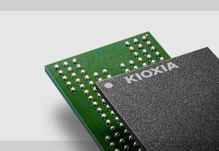
Kioxia and Western Digital Could Announce Merger This Month

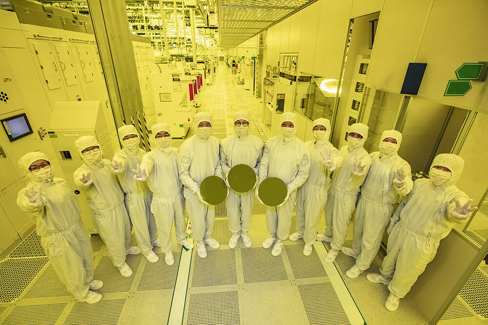
According to Kyodo News, Japanese chip manufacturer Kioxia and its U.S. counterpart Western Digital are reportedly on the verge of finalizing a merger agreement, aiming to create the world's largest producer of memory chips. The merger plan involves establishing a holding company to consolidate their operations for producing NAND flash memory chips, with the announcement reportedly coming this month. The merged entity is expected to be listed on the Nasdaq stock exchange in the United States. As the global semiconductor market contends with competitive pressures and fluctuating demand, the merger is seen as a strategic move to enhance the combined market position of both companies.

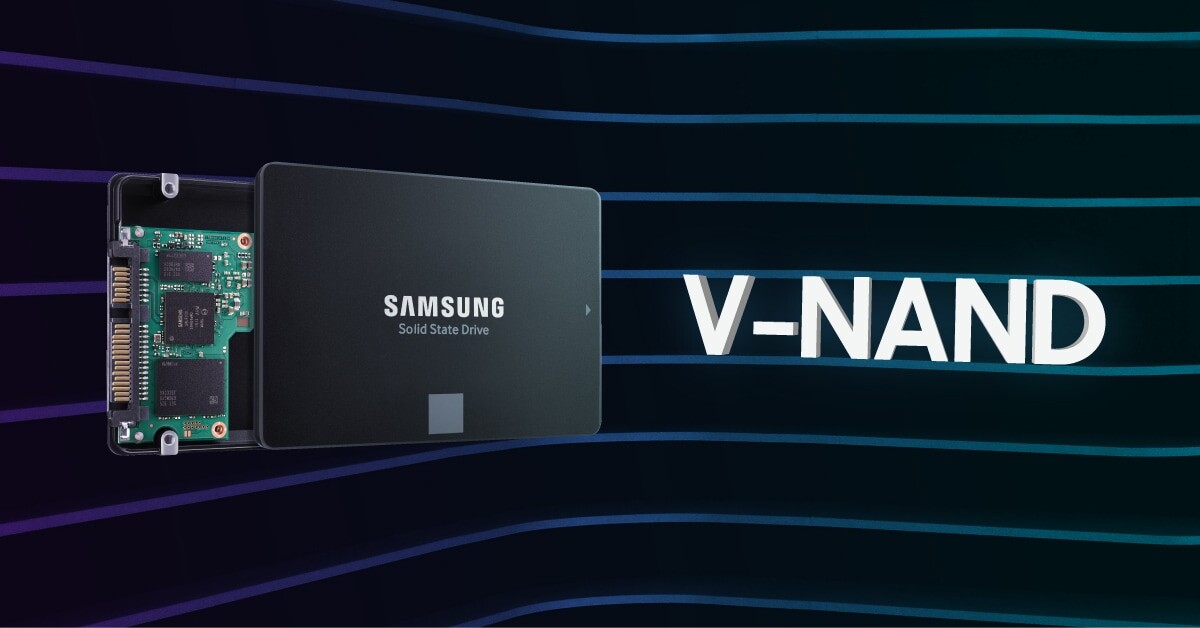
Western Digital shareholders are anticipated to hold a majority stake in the new entity, with Kioxia's shareholders, including Toshiba Corporation, owning the remaining stake. The move is poised to give the newly formed company a combined market share of 35.4 percent in NAND memory chips as of March, surpassing South Korea's Samsung, the current leader, with 34.3 percent. However, the merger's ultimate approval hinges on regulators' decisions, including those in China, as semiconductors have become increasingly integral to global economic security. Major Japanese banks, including MUFG Bank and the state-backed Development Bank of Japan, are contemplating loans of up to approximately 1.9 trillion yen (about $12.7 billion) to facilitate the merger.

Samsung Electronics Holds Memory Tech Day 2023 Unveiling New Innovations To Lead the Hyperscale AI Era

Samsung Electronics Co., Ltd., a world leader in advanced memory technology, today held its annual Memory Tech Day, showcasing industry-first innovations and new memory products to accelerate technological advancements across future applications—including the cloud, edge devices and automotive vehicles.

Attended by about 600 customers, partners and industry experts, the event served as a platform for Samsung executives to expand on the company's vision for "Memory Reimagined," covering long-term plans to continue its memory technology leadership, outlook on market trends and sustainability goals. The company also presented new product innovations such as the HBM3E Shinebolt, LPDDR5X CAMM2 and Detachable AutoSSD.

Samsung V-NAND with 300+ Layers is Coming in 2024, Notes Company Executive

Jung-Bae Lee, President and Head of Memory Business of Samsung Electronics, the world's largest NAND memory supplier, has noted in the blog post that Samsung plans to develop its 9th Generation V-NAND memory with over 300 layers, aiming for mass production in 2024. Samsung's V-NAND uses a double-stack structure and is expected to have more active layers than its competitors' 3D NAND memory, such as SK Hynix's forthcoming 321-layer memory. The increase in layers allows Samsung to enhance storage density and performance in its future 3D NAND devices, focusing on input/output (I/O) speed. While the specific performance details of Samsung's 9th Generation V-NAND remain undisclosed, the memory is expected to be used in next-generation PCIe SSDs with the PCIe 5.0 standard.

Jung-Bae Lee has noted: "New structural and material innovations will be critical in the upcoming era of sub-10-nanometer (nm) DRAM and 1,000-layer vertical V-NAND. As such, we are developing 3D stacked structures and new materials for DRAM while increasing layer count, decreasing height, and minimizing cell interference for V-NAND." The 9th installment of V-NAND, scheduled for 2024, is utilizing 11 nm-class DRAM. Additionally, the blog post reassures the commitment to CXL Memory Modules (CMM), which will enable the composable infrastructure of next-generation systems, especially with high-capacity SSDs powered by V-NAND.

Samsung Notes: HBM4 Memory is Coming in 2025 with New Assembly and Bonding Technology

According to the editorial blog post published on the Samsung blog by SangJoon Hwang, Executive Vice President and Head of the DRAM Product & Technology Team at Samsung Electronics, we have information that High-Bandwidth Memory 4 (HBM4) is coming in 2025. In the recent timeline of HBM development, we saw the first appearance of HBM memory in 2015 with the AMD Radeon R9 Fury X. The second-generation HBM2 appeared with NVIDIA Tesla P100 in 2016, and the third-generation HBM3 saw the light of the day with NVIDIA Hopper GH100 GPU in 2022. Currently, Samsung has developed 9.8 Gbps HBM3E memory, which will start sampling to customers soon.

However, Samsung is more ambitious with development timelines this time, and the company expects to announce HBM4 in 2025, possibly with commercial products in the same calendar year. Interestingly, the HBM4 memory will have some technology optimized for high thermal properties, such as non-conductive film (NCF) assembly and hybrid copper bonding (HCB). The NCF is a polymer layer that enhances the stability of micro bumps and TSVs in the chip, so memory solder bump dies are protected from shock. Hybrid copper bonding is an advanced semiconductor packaging method that creates direct copper-to-copper connections between semiconductor components, enabling high-density, 3D-like packaging. It offers high I/O density, enhanced bandwidth, and improved power efficiency. It uses a copper layer as a conductor and oxide insulator instead of regular micro bumps to increase the connection density needed for HBM-like structures.

OLED Monitor Shipments Predicted to Soar by 323% in 2023; 2024 Shipments Expected to Surpass One Million Units

TrendForce reports that the ever-expanding dimensions of OLED products, combined with the ambitious plans of several top-tier brands, mean that 2023 could see OLED monitor shipments hitting a staggering 508,000 units—an astronomical YoY surge of 323%. Come 2024, the OLED landscape will be richer with more diverse product sizes and specifications. Add to that the debut of the 27-inch and 31.5-inch OLED panels by two leading Korean panel makers, and the arena is set for a showdown. Such dynamics are predicted to catapult OLED monitor shipments past the coveted one million unit threshold.

In terms of market share, Samsung is on track for a spirited push in OLED monitor shipments in 2H23, potentially capturing a market share of 27%—echoing LGE's performance. Not to be left behind, Dell is ardently pushing its 34-inch offering, hoping to clinch a market presence above 20%. Meanwhile, ASUS, having strategically positioned itself in the OLED monitor sector recently, is eyeing a market share nearing 9% this year.

Samsung Briefly Details Exynos 2400 SoC with Xclipse 940 AMD RDNA 3 GPU at LSI Tech Day 2023 Event

Samsung Electronics Co., Ltd., a world leader in advanced semiconductor technology, today unveiled its latest innovations in analog and logic semiconductor technologies and outlined its blueprint for upcoming technological advancements at its inaugural Samsung System LSI Tech Day 2023 event. Attended by approximately 300 customers and partners at its Samsung Semiconductor U.S. headquarters, the event featured tech sessions led by Samsung executives, covering a wide range of topics from System LSI humanoids to AI and the company's R&D endeavors in the U.S. 11In the opening keynote, Samsung emphasized the company's vision to lead hyper-intelligent, hyper-connected and hyper-data technologies in the Fourth Industrial Revolution era with its comprehensive logic solutions uniquely tailored for various industries.

"Generative AI has quickly emerged as perhaps the most significant trend of the year, demanding more powerful foundational technologies to process data and bring AI to life," said Yong-In Park, President and Head of System LSI Business at Samsung Electronics. "We are paving the path toward a new era of proactive AI, leveraging our Samsung System LSI Humanoid platform, which seamlessly converges our capabilities across a broad spectrum of logic semiconductors, from powerful computational IPs, connectivity solutions to sensors emulating the main five human senses."

Samsung and TSMC Reportedly Struggling with 3 nm Yields

According to Korean business news publication ChosunBiz, both Samsung and TSMC are struggling with their 3 nm node yields. The two companies have different approaches to their 3 nm nodes, with Samsung using GAA FET (Gate All Around), whereas TSMC is continuing with its FinFET technology. That said, TSMC has at least five known 3 nm nodes, of which two should be in production by now, assuming N3E has proved to be reliable enough to kick off. Samsung on the other hand has three known 3 nm nodes, with only one in production so far, called 3GAE.

ChosunBiz reports that neither company is getting the kind of yields that you'd expect from a node that should have been in volume production for around a year by now, with Samsung apparently being somewhat better than TSMC. At 60 and 50 percent respectively, neither Samsung nor TSMC are anywhere near decent yields. Anything below 70 percent is considered very poor and even the 60 percent claim in Samsungs case, is apparently limited to some kind of Chinese mining ASIC and doesn't include the SRAM you find in most modern processors. ChosunBiz also mentions a source familiar with Samsung's foundry business who mentions a yield closer to 50 percent for the company. The same source also mentions that Samsung needs to reach at least 70 percent yield to be able to attract major customers to its 3 nm node.

Second Half Utilization Rate for 8-inch Production Capacity Expected to Drop to 50-60%; Chilly Demand Prospects Until 1Q24

TrendForce research indicates that in 1H23, the utilization rate of 8-inch production capacity primarily benefited from sporadic inventory restocking orders for Driver ICs in the second quarter. Additionally, wafer foundries initiated pricing strategies to encourage clients into early orders, offering solid backup. However, in 2H23, persistent macroeconomic and inventory challenges led to the evaporation of an anticipated demand surge.

Meanwhile, stockpiles in automotive and industrial control segments grew after meeting initial shortages, tempering demand. Under fierce price competition from PMIC leader Texas Instruments (TI), inventory reductions for Fabless and other IDMs were drastically inhibited. With IDMs ushering in output from their new plants and pulling back outsourced orders, this compounded reductions to wafer foundries. This dynamic saw 8-inch production capacity utilization dipping to 50-60% in the second half of the year. Both Tier 1 and Tier 2/3 8-inch wafer foundries saw a more lackluster capacity utilization performance compared to the first half of the year.

Samsung Announces Portable Solid State Drive (SSD) T9

Samsung Electronics, a global leader in advanced memory technology, today announced the release of its latest lineup of the T-series, the Portable Solid State Drive (SSD) T9. With its stylish and portable design, the T9 is built to keep data safe while on-the-go, empowering users with fast transfer speeds and ample storage, and providing the reliability and convenience they need.

"With advances in high-resolution photos and the rising popularity of 4K videos, professional content creators now face the necessity of transferring large amounts of data on a frequent basis," said Hangu Sohn, Vice President of Memory Brand Product Biz Team at Samsung Electronics. "The T9 offers a solution for professionals to alleviate the challenges that come with managing their data, and Samsung will continue to provide optimized memory solutions that enable professionals to fully concentrate on achieving their creative potential."

Tenstorrent Selects Samsung Foundry to Manufacture Next-Generation AI Chiplet

Tenstorrent, a company that sells AI processors and licenses AI and RISC-V IP, announced today that it selected Samsung Foundry to bring Tenstorrent's next generation of AI chiplets to market. Tenstorrent builds powerful RISC-V CPU and AI acceleration chiplets, aiming to push the boundaries of compute in multiple industries such as data center, automotive and robotics. These chiplets are designed to deliver scalable power from milliwatts to megawatts, catering to a wide range of applications from edge devices to data centers.

To ensure the highest quality and cutting-edge manufacturing capabilities for its chiplet, Tenstorrent has selected Samsung's Foundry Design Service team, known for their expertise in silicon manufacturing. The chiplets will be manufactured using Samsung's state-of-the-art SF4X process, which boasts an impressive 4 nm architecture.

TSMC Announces Breakthrough Set to Redefine the Future of 3D IC

TSMC today announced the new 3Dblox 2.0 open standard and major achievements of its Open Innovation Platform (OIP) 3DFabric Alliance at the TSMC 2023 OIP Ecosystem Forum. The 3Dblox 2.0 features early 3D IC design capability that aims to significantly boost design efficiency, while the 3DFabric Alliance continues to drive memory, substrate, testing, manufacturing, and packaging integration. TSMC continues to push the envelope of 3D IC innovation, making its comprehensive 3D silicon stacking and advanced packaging technologies more accessible to every customer.

"As the industry shifted toward embracing 3D IC and system-level innovation, the need for industry-wide collaboration has become even more essential than it was when we launched OIP 15 years ago," said Dr. L.C. Lu, TSMC fellow and vice president of Design and Technology Platform. "As our sustained collaboration with OIP ecosystem partners continues to flourish, we're enabling customers to harness TSMC's leading process and 3DFabric technologies to reach an entirely new level of performance and power efficiency for the next-generation artificial intelligence (AI), high-performance computing (HPC), and mobile applications."

Samsung Electronics' Industry-First LPCAMM Ushers in Future of Memory Modules

Samsung Electronics, a world leader in advanced memory technology, today announced that it has developed the industry's first Low Power Compression Attached Memory Module (LPCAMM) form factor, which is expected to transform the DRAM market for PCs and laptops - and potentially even data centers. Samsung's groundbreaking development for its 7.5 gigabits-per-second (Gbps) LPCAMM has completed system verification through Intel's platform. Historically, PCs and laptops have conventionally used LPDDR DRAM or DDR-based So-DIMMs. While LPDDR is compact, it's permanently attached to the motherboard, making it challenging to replace during repairs or upgrades. On the other hand, So-DIMMs can be attached or detached easily but have limitations with performance and other physical features.

LPCAMM overcomes the shortcomings of both LPDDR and So-DIMMs, addressing the increased demand for more efficient yet compact devices. Being a detachable module, LPCAMM offers enhanced flexibility for PC and laptop manufacturers during the production process. Compared to So-DIMM, LPCAMM occupies up to 60% less space on the motherboard. This allows more efficient use of devices' internal space while also improving performance by up to 50% and power efficiency by up to 70%. LPDDR's power-saving features have made it an attractive option for servers, since it could potentially improve total cost of operation (TCO) efficiency. However, using LPDDR can create operational difficulties such as the need to replace the entire motherboard when upgrading a server's DRAM specifications. LPCAMM offers a solution to these challenges, creating significant potential for it to become the solution of choice for future data centers and servers.

Samsung T9 Portable SSDs Listed by Retailers

Samsung seems to be preparing follow ups to its current selection of Portable T7 SSDs—the series debuted back in early 2020, so a couple of successors are more than due. Last week TechRadar started to pick up on various retail listings popping up in Australia, France and the Netherlands. This information was posted online prematurely and by mistake—the involved organizations have since removed entries from their web stores. Samsung's Dutch division has been slow to respond, and its portal for a "MU-PG2T0B" model is still active (at the time of writing). France's Grosbill and P12.fr had listings for two T9 variants (1 TB and 2 TB configurations) sporting the aforementioned product code. Similar details appeared over in Australia, courtesy of the Microboss site. One of the French e-tailer spec sheets mentioned that Samsung's T9 SSD read and write speeds maxed out at 2 GB/s.

TechRadar believes that Samsung will be blowing out current T7 models during November's Black Friday sales week, in anticipation of clearing the way for all things T9. The publication managed to catch some (likely) placeholder prices from its sources, prior to removal: "There's also every chance it could be cheaper at launch than the T7, with PC12.fr retailing the T9 SSD for €236.52 including VAT (roughly $250) and Gosbill Pro retailing the device for just €199 (roughly $215) - though it's unclear if this is inclusive of taxes." There is also speculation regarding the integration of Thunderbolt 4 connectivity, since the older T7 generation relies on the preceding standard.

Samsung and AMD Collaborate To Advance Network Transformation With vRAN

Samsung Electronics today announced a new collaboration with AMD to advance 5G virtualized RAN (vRAN) for network transformation. This collaboration represents Samsung's ongoing commitment to enriching vRAN and Open RAN ecosystems to help operators build and modernize mobile networks with unmatched flexibility and optimized performance. The two companies have completed several rounds of tests at Samsung's lab to verify high-capacity and telco-grade performance using FDD bands and TDD Massive MIMO wide-bands, while significantly reducing power consumption. In this joint collaboration, Samsung used its versatile vRAN software integrated with the new AMD EPYC 8004 processors, focused on telco and intelligent edge. During technical verification, the EPYC 8004 processors combined with Samsung's vRAN solutions delivered optimized cell capacity per server as well as high power efficiency.

"This technical collaboration demonstrates Samsung's commitment to delivering network flexibility and high performance for service providers by building a larger vRAN and Open RAN ecosystem," said Henrik Jansson, Vice President and Head of SI Business Group, Networks Business at Samsung Electronics. "Samsung has been at the forefront of unleashing the full potential of 5G vRAN technology to meet rising demands, and we look forward to collaborating with industry leaders like AMD to provide operators the capabilities to transform their networks."

TSMC Could Delay 2 nm Mass Production to 2026

According to TechNews.tw, TSMC could postpone its 2 nm semiconductor manufacturing node for 2026. If the rumors about TSMC's delayed 2 nm production schedule are accurate, the implications could reverberate throughout the semiconductor industry. TSMC's alleged hesitancy could be driven by multiple factors, including the architectural shift from FinFET to Gate-All-Around (GAA) and potential challenges related to scaling down to 2 nm. The company is a crucial player in this space, and a delay could offer opportunities for competitors like Samsung, which has already transitioned to GAA transistor architecture for its 3 nm chips. Given the massive demand for advanced nodes due to the rise of AI, IoT, and other next-gen technologies, it is surprising to hear "sluggish" demand reports.

However, it's also possible that it's too early for customers to make firm commitments for 2025 and beyond. TSMC has dismissed these rumors, stating that construction is progressing according to plan, which includes having 2 nm pilot run in 2024, and mass production in the second half of 2025.. Despite this, any delay in TSMC's roadmap could serve as a catalyst for shifts in market dynamics. Companies that rely heavily on TSMC's advanced nodes might need to reassess their timelines and strategies. Moreover, if Samsung can capitalize on this opportunity, it could somewhat level the playing field. As of now, though, it's essential to approach these rumors with caution until more concrete information becomes available.

Nintendo Switch 2 to Feature NVIDIA Ampere GPU with DLSS

The rumors of Nintendo's next-generation Switch handheld gaming console have been piling up ever since the competition in the handheld console market got more intense. Since the release of the original Switch, Valve has released Steam Deck, ASUS made ROG Ally, and others are also exploring the market. However, the next-generation Nintendo Switch 2 is closer and closer, as we have information about the chipset that will power this device. Thanks to Kepler_L2 on Twitter/X, we have the codenames of the upcoming processors. The first generation Switch came with NVIDIA's Tegra X1 SoC built on a 20 nm node. However, later on, NVIDIA supplied Nintendo with a Tegra X1+ SoC made on a 16 nm node. There were no performance increases recorded, just improved power efficiency. Both of them used four Cortex-A57 and four Cortex-A53 cores with GM20B Maxwell GPUs.

For the Nintendo Switch 2, NVIDIA is said to utilize a customized variant of NVIDIA Jetson Orin SoC for automotive applications. The reference Orin SoC carries a codename T234, while this alleged adaptation has a T239 codename; the version is most likely optimized for power efficiency. The reference Orin design is a considerable uplift compared to the Tegra X1, as it boasts 12 Cortex-A78AE cores and LPDDR5 memory, along with Ampere GPU microarchitecture. Built on Samsung's 8 nm node, the efficiency would likely yield better battery life and position the second-generation Switch well among the now extended handheld gaming console market. However, including Ampere architecture would also bring technologies like DLSS, which would benefit the low-power SoC.

Q2 NAND Flash Revenue Up 7.4%, Anticipated to Exceed 3% Growth in Q3

TrendForce's latest research paints a vivid picture: Q2 saw the NAND Flash market still grappling with lackluster demand and being significantly outpaced by supply. The ASP of NAND Flash also took a hit, tumbling 10-15%. Nevertheless, there was a silver lining as bit shipments grew by 19.9% QoQ from a low baseline in 1Q23. To sum up, the Q2 landscape of the NAND Flash sector witnessed a 7.4% QoQ growth in revenue, reaching US$9.338 billion.

From Q2, Samsung began reining in production with a further squeeze expected for the third quarter. With inventories set to thin out, price hikes loom on the horizon, possibly offering a remedy to the chronic supply-demand imbalance. Yet, a crowded supplier landscape in the NAND Flash sector means that many players, faced with hefty inventories, will likely continue aggressive sales into Q3. Forecasts suggests a deceleration in ASP decline for NAND Flash products in Q3 to 5-10%. Riding the stockpiling momentum for the high season, bit shipments are set to rise, propelling Q3 revenue growth past the 3% threshold.

Intel's Meteor Lake CPU Breaks Ground with On-Package LPDDR5X Memory Integration

During a recent demonstration, Intel showcased its cutting-edge packaging technologies, EMIB (embedded multi-die interconnect bridge) and Foveros, unveiling the highly-anticipated Meteor Lake processor with integrated LPDDR5X memory. This move appears to align with Apple's successful integration of LPDDR memory into its M1 and M2 chip packages. At the heart of Intel's presentation was the quad-tile Meteor Lake CPU, leveraging Foveros packaging for its chiplets and boasting 16 GB of Samsung's LPDDR5X-7500 memory. Although the specific CPU configuration remains undisclosed, the 16 GB of integrated memory delivers a remarkable peak bandwidth of 120 GB/s, outperforming traditional memory subsystems using DDR5-5200 or LPDDR5-6400.

Nevertheless, this approach comes with trade-offs, such as the potential for system-wide failure if a memory chip malfunctions, limited upgradeability in soldered-down configurations, and the need for more advanced cooling solutions to manage CPU and memory heat. While Apple pioneered on-package LPDDR memory integration in client CPUs, Intel has a history of using package-on-package DRAM with its Atom-branded CPUs for tablets and ultrathin laptops. While this approach simplifies manufacturing, enabling slimmer notebook designs, it curtails configuration flexibility. We are yet to see if big laptop makers such as Dell, HP, and Asus, take on this design in the coming months.

Samsung Announces 4 TB SSD 990 PRO Series

Samsung Electronics Co., Ltd., a world leader in advanced memory technology, today announced the release of a new 4-terabyte (TB) offering in its SSD 990 PRO series. The 990 PRO series is a lineup of high-performance PCIe 4.0 SSDs powered by Samsung's eighth-generation V-NAND (V8) technology and enhanced proprietary controller. Offering blazing-fast speeds and ultimate power efficiency, the 990 PRO series is optimized for massive data volumes, such as 3D/4K graphics work, data analytics and high-quality games, making it the ideal SSD for today's PCs, laptops, game consoles and computing systems. With improved total bytes written (TBW) ratings of up to 2,400 TB, the 990 PRO series ensures increased SSD reliability and longevity, ideal for those with highly demanding workloads and large storage capacity needs.

"Today's gamers and creative professionals require high-capacity, high-performance SSDs and Samsung's new 4 TB SSD 990 PRO is the perfect storage solution to meet their needs," said Hangu Sohn, Corporate Vice President of the Memory Brand Product Biz Team at Samsung Electronics. "As the demand for high-resolution content and ultra-fast data-processing speeds continues to grow, high-performance NVMe storage has become a core requirement."

Top Ten Semiconductor Foundries Report a 1.1% Quarterly Revenue Decline in 2Q23, Anticipated to Rebound in 3Q23

TrendForce reports an interesting shift in the electronics landscape: dwindling inventories for TV components, along with a surging mobile repair market that's been driving TDDI demand, have sparked a smattering of urgent orders in the Q2 supply chain. These last-minute orders have served as pivotal lifelines, propping up Q2 capacity utilization and revenue for semiconductor foundries. However, the adrenaline rush from these stop-gap orders may be a short-lived phenomenon and is unlikely to be carried over into the third quarter.

On the other hand, demand for staple consumer products like smartphones, PCs, and notebooks remains sluggish, perpetuating a slump in the use of expensive, cutting-edge manufacturing processes. At the same time, traditionally stable sectors—automotive, industrial control, and servers—are undergoing inventory correction. The confluence of these trends has resulted in a sustained contraction for the world's top ten semiconductor foundries. Their global revenue declined by approximately 1.1% for the quarter, amounting to a staggering US$26.2 billion.

Arm Prepares for IPO: Apple, NVIDIA, Intel, and Samsung are Strategic Partners

Arm's impending IPO, valued between $60 billion and $70 billion, has reportedly garnered substantial backing from industry giants such as Apple, NVIDIA, Intel, and Samsung, as per sources cited in a Bloomberg report. This much-anticipated public offering serves as a litmus test for investor interest in new chip-related stocks and could reshape the tech industry landscape. While the information remains unofficial, it underscores the significant support Arm has received from major licensees, including Apple, AMD, Cadence, Intel, Google, NVIDIA, Samsung, and Synopsys, with each potentially contributing between $25 million and $100 million, a testament to their confidence in Arm's future prospects. Originally, SoftBank aimed to raise $8 billion to $10 billion through the IPO, but a strategic shift to retain a larger Arm stake revised the target to $5 billion to $7 billion.

This IPO's success holds paramount importance for SoftBank and its CEO, Masayoshi Son, particularly following the Vision Fund's substantial $30 billion loss in the previous fiscal year. Masayoshi Son is reportedly committed to maintaining significant control over Arm, planning to release no more than 10% of the company's shares during this initial phase, aligning with SoftBank's recent acquisition of the Vision Fund's Arm stake and reinforcing their belief in Arm's long-term potential. Arm has enlisted renowned global financial institutions such as Barclays, Goldman Sachs Group, JPMorgan Chase & Co., and Mizuho Financial Group to prepare for the IPO, highlighting the widespread interest in the offering and the anticipated benefits for these financial institutions.

Samsung Electronics Unveils Industry's Highest-Capacity 12nm-Class 32Gb DDR5 DRAM

collaboration with diverse industries and support various applications
Samsung Electronics, a world leader in advanced memory technology, today announced that it has developed the industry's first and highest-capacity 32-gigabit (Gb) DDR5 DRAM using 12 nanometer (nm)-class process technology. This achievement comes after Samsung began mass production of its 12 nm-class 16Gb DDR5 DRAM in May 2023. It solidifies Samsung's leadership in next-generation DRAM technology and signals the next chapter of high-capacity memory.

"With our 12 nm-class 32Gb DRAM, we have secured a solution that will enable DRAM modules of up to 1-terabyte (TB), allowing us to be ideally positioned to serve the growing need for high-capacity DRAM in the era of AI (Artificial Intelligence) and big data," said SangJoon Hwang, Executive Vice President of DRAM Product & Technology at Samsung Electronics. "We will continue to develop DRAM solutions through differentiated process and design technologies to break the boundaries of memory technology."

Suppliers Successfully Hike Wafer Contract Prices, Triggering Short-Term Surge in NAND Spot Market

Recently, the spot market for NAND Flash chips has seen a rise in active price inquiries for certain products, a movement driven by successful increases in wafer contract prices. TrendForce reports this uptick primarily stems from negotiations in late August between NAND Flash suppliers and key Chinese module makers. These discussions led to a new wafer contract that successfully boosted the price of 512 Gb wafers by approximately 10%.

Other suppliers have also raised prices for their comparable products, signaling a shift in supplier sentiment: they are now less inclined to finalize deals at lower prices. This change has contributed to a short-term surge in the wafer spot market. Nevertheless, whether this surge in procurement is supported by actual end-user demand remains uncertain, as these orders have arisen in reaction to adjustments in supply-side pricing.

Global Enterprise SSD Revenue Hits New Low in Q2 at US$1.5 Billion, Peak Season Growth Expected to Fall Short of Forecasts

TrendForce research reveals that, due to the impacts of high inflation and economic downturn, CSPs are adopting more conservative strategies when it comes to capital expenditure and consistently reducing their annual server demand forecasts. Currently, CSPs in China have reported a decline in cloud orders compared to last year, leading to a subsequent decrease in annual procurement volumes for enterprise SSDs. In North America, some clients have postponed mass production timelines for new server platforms while ramping up investments in AI servers. These factors have resulted in enterprise SSD orders falling below expectations. Consequently, global enterprise SSD revenue hit an all-time low in the second quarter, totaling just $1,500 million—a QoQ decrease of 24.9%.

Demand for AI servers remains strong in the third quarter, while orders and shipment momentum for general-purpose servers have yet to show signs of recovery. This continues to put pressure on the purchasing volume of enterprise SSDs, and annual bit volume is expected to be lower than last year. Meanwhile, vendors have once again reduced capacity utilization to slow down inventory growth. Server customers still maintain high inventory levels, and their purchasing momentum remains insufficient. This is expected to lead to an approximate 15% QoQ decline in the average price of enterprise SSDs in the third quarter, which may further result in a lackluster revenue performance for the peak season.

Galaxy Buds2 Pro Evolves LE Audio Capabilities, Bringing New Auracast to Samsung Smart TV

Samsung Electronics today announced new software updates to Galaxy Buds2 Pro and Samsung Smart TVs, reshaping the audio experiences across even more connected devices. The new updates extend LE Audio capabilities to Samsung TVs with Auracast broadcast audio technology, enabling rich and complex audio transmission to nearby Bluetooth devices.

LE Audio, an advanced Bluetooth audio standard, broadens the spectrum of audio experiences to deliver more complex and richer sound that goes beyond providing better-sounding music, but also allows users to share sound with others as they personally experience it. As a pioneer of innovative technologies, Samsung has been leveraging new LE Audio-based features that further elevate sound experiences, including 360 Audio Recording, enabling Galaxy smartphone users to capture sound on video precisely as they hear it without the need for professional equipment. Additionally, the select Galaxy Book3 devices offer a crystal clear listening experience with improved latency—perfect for immersive gaming and multimedia consumption.
Return to Keyword Browsing
May 21st, 2024 20:20 EDT change timezone

New Forum Posts

Popular Reviews

Controversial News Posts