News Posts matching #Sapphire Rapids

Return to Keyword Browsing

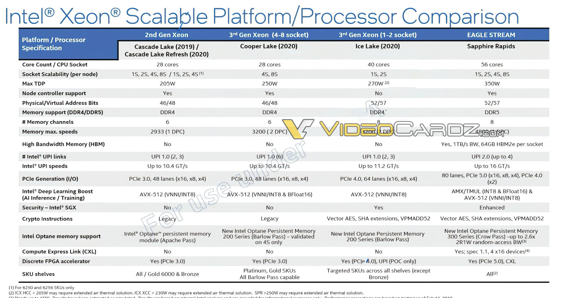
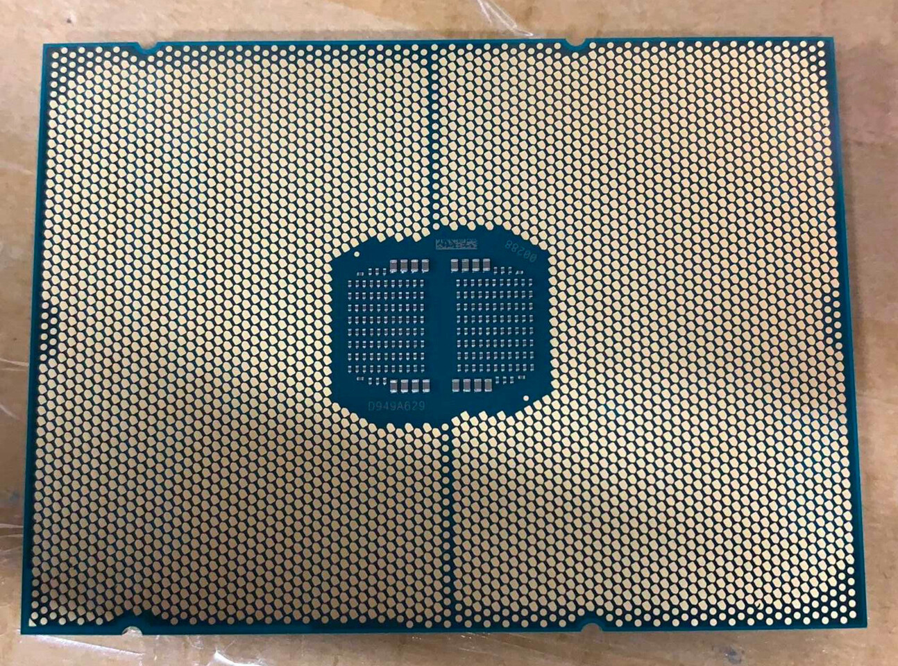
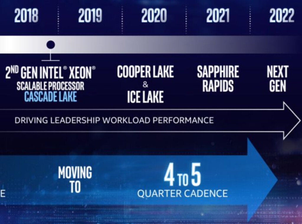
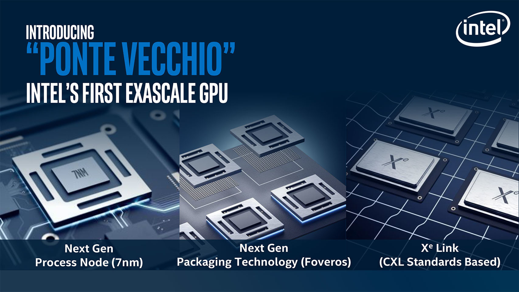
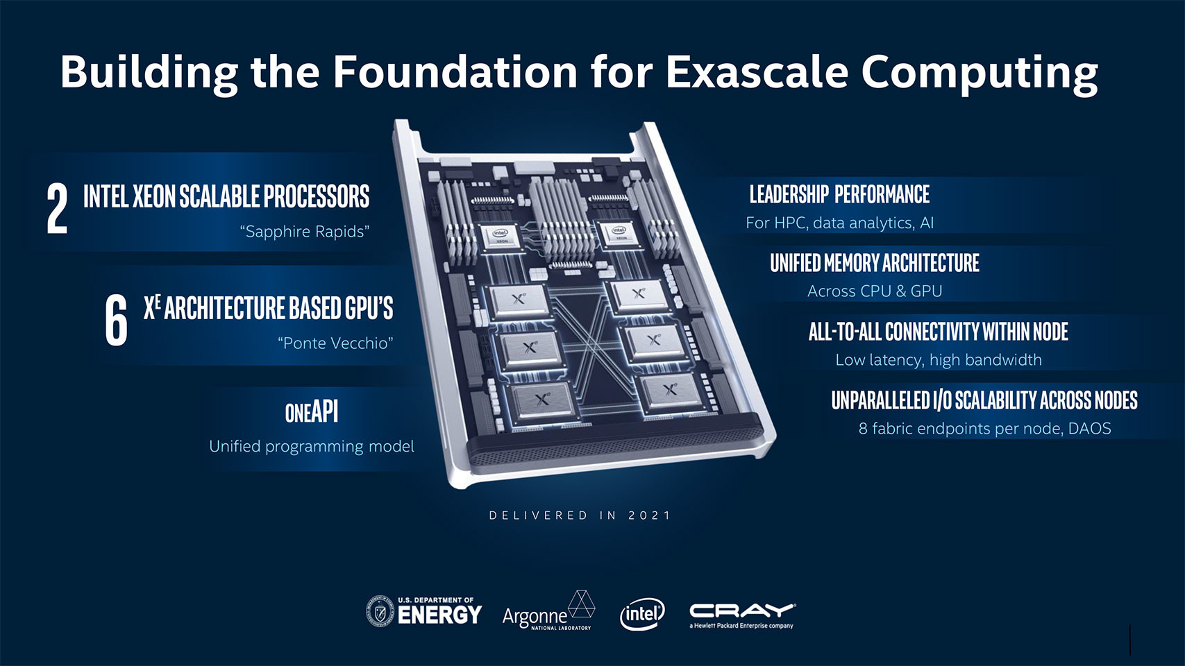
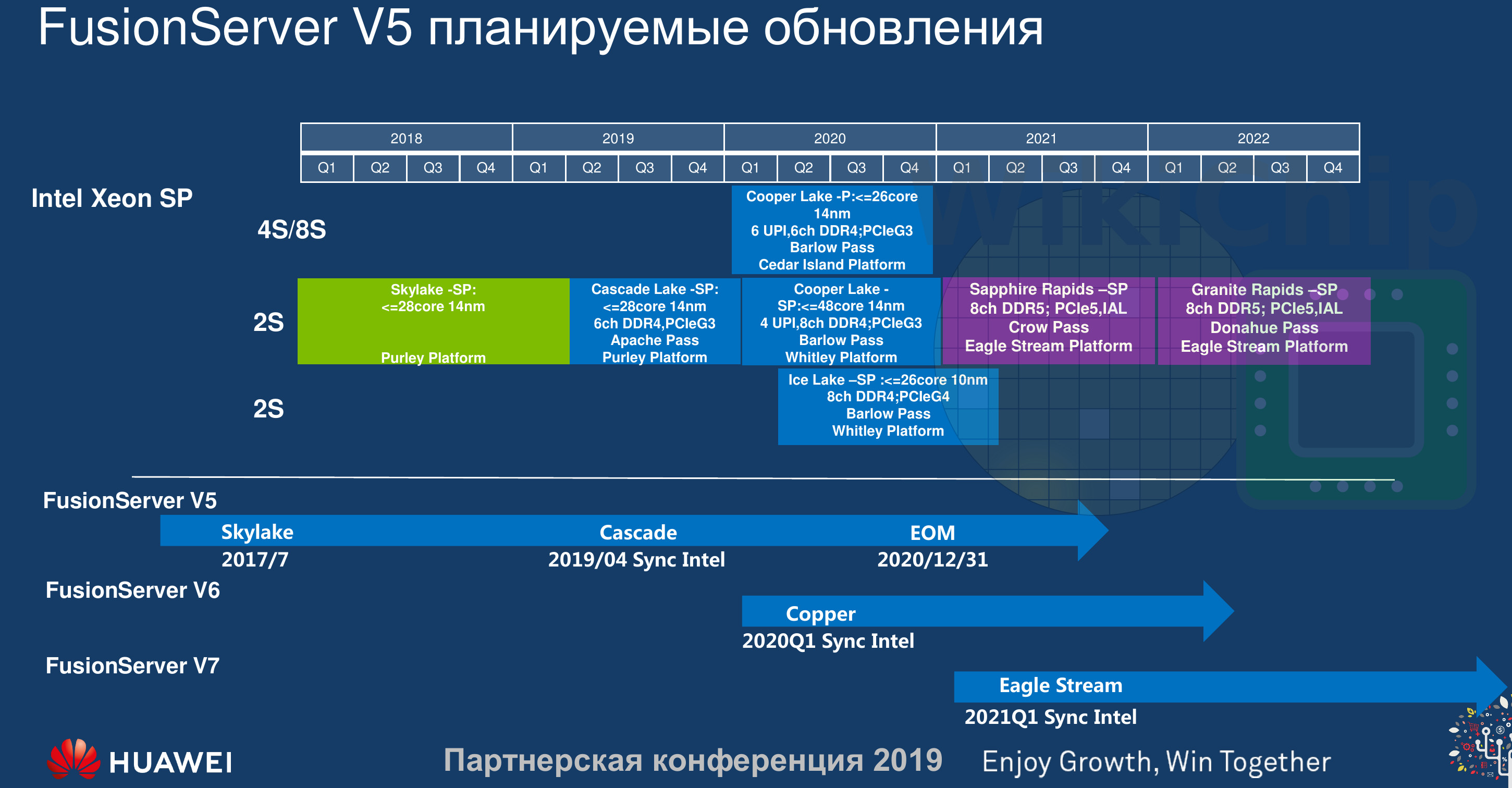
Intel's Upcoming Sapphire Rapids Server Processors to Feature up to 56 Cores with HBM Memory

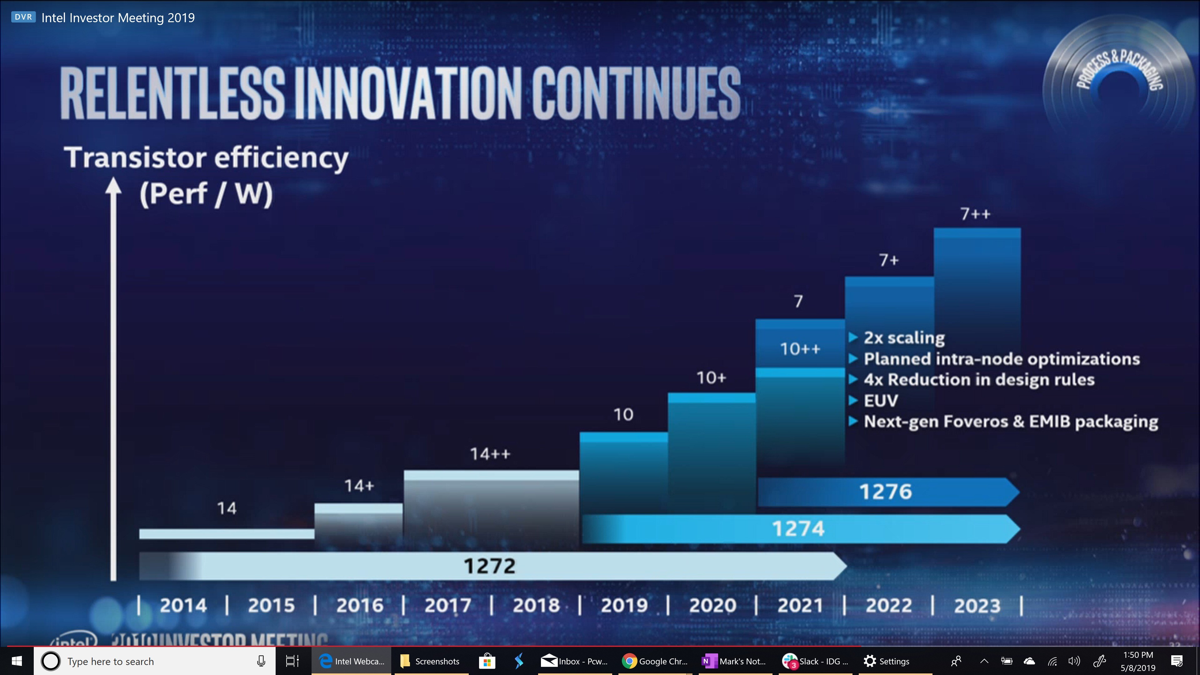
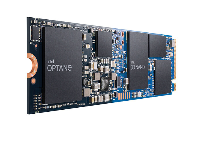
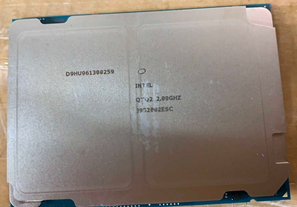
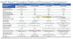
Intel has just launched its Ice Lake-SP lineup of Xeon Scalable processors, featuring the new Sunny Cove CPU core design. Built on the 10 nm node, these processors represent Intel's first 10 nm shipping product designed for enterprise. However, there is another 10 nm product going to be released for enterprise users. Intel is already preparing the Sapphire Rapids generation of Xeon processors and today we get to see more details about it. Thanks to the anonymous tip that VideoCardz received, we have a bit more details like core count, memory configurations, and connectivity options. And Sapphire Rapids is shaping up to be a very competitive platform. Do note that the slide is a bit older, however, it contains useful information.

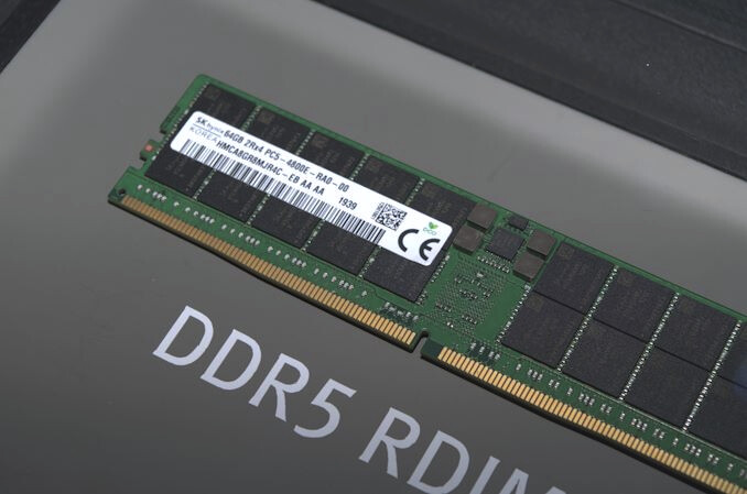
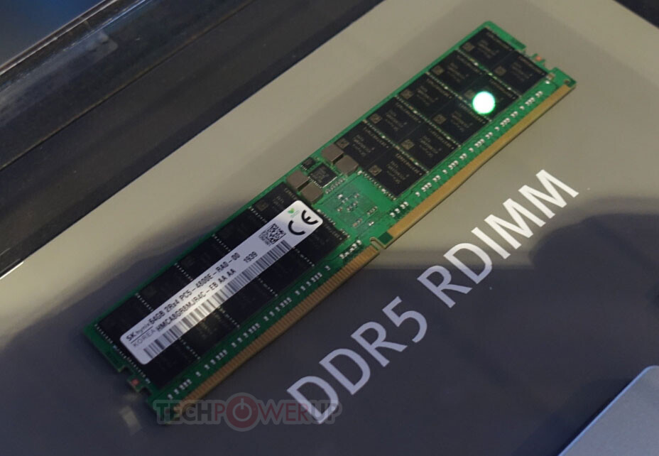
The lineup will top at 56 cores with 112 threads, where this processor will carry a TDP of 350 Watts, notably higher than its predecessors. Perhaps one of the most interesting notes from the slide is the department of memory. The new platform will make a debut of DDR5 standard and bring higher capacities with higher speeds. Along with the new protocol, the chiplet design of Sapphire Rapids will bring HBM2E memory to CPUs, with up to 64 GBs of it per socket/processor. The PCIe 5.0 standard will also be present with 80 lanes, accompanying four Intel UPI 2.0 links. Intel is also supposed to extend the x86_64 configuration here with AMX/TMUL extensions for better INT8 and BFloat16 processing.

Silicon Motion: PCIe 5.0 SSD Controller to Arrive Next Year

With the debut of PCIe 4.0 standard, SSD manufacturers have started launching a new generation of storage devices, with unseen speeds before. Today's PCIe 4.0 SSDs can reach up to 8.0 GB/s reads and writes, all thanks to the bandwidth-heavy PCIe protocol. However, enterprise workloads are always requiring more and more bandwidth to satisfy their needs. Data is being moved in immense quantities and faster hardware is always welcome. The previous PCIe 4.0 standard is about to kneel to its successor - PCIe 5.0 protocol. Having double the amount of bandwidth, the new standard is set to bring unseen speeds.

The PCIe 5.0 protocol offers 32 GT/s per lane, making up to 64 GB/s in the full x16 implementation. However, when it comes to SSDs, as they use x4 lanes, it will increase the maximum speed to 16 GB/s, doubling the previous bandwidth. Silicon Motion, the maker of NAND flash controllers, has announced that the company is going to debut a PCIe 5.0 controller next year. "We are excited about enterprise-grade PCIe Gen5 controller, which we will have taped out early next year and sample in the second half of 2022", said Wallace Kuo, chief executive of Silicon Motion, during a conference call. Launching just in time to pair with Intel's Sapphire Rapids Xeon processors that support the PCIe 5.0 protocol, Silicon Motion is probably expecting to grab its market share there.

Microchip Announces World's First PCI Express 5.0 Switches

Applications such as data analytics, autonomous-driving and medical diagnostics are driving extraordinary demands for machine learning and hyperscale compute infrastructure. To meet these demands, Microchip Technology Inc. today announced the world's first PCI Express (PCIe) 5.0 switch solutions—the Switchtec PFX PCIe 5.0 family—doubling the interconnect performance for dense compute, high speed networking and NVM Express (NVMe ) storage. Together with the XpressConnect retimers, Microchip is the industry's only supplier of both PCIe Gen 5 switches and PCIe Gen 5 retimer products, delivering a complete portfolio of PCIe Gen 5 infrastructure solutions with proven interoperability.

"Accelerators, graphic processing units (GPUs), central processing units (CPUs) and high-speed network adapters continue to drive the need for higher performance PCIe infrastructure. Microchip's introduction of the world's first PCIe 5.0 switch doubles the PCIe Gen 4 interconnect link rates to 32 GT/s to support the most demanding next-generation machine learning platforms," said Andrew Dieckmann, associate vice president of marketing and applications engineering for Microchip's data center solutions business unit. "Coupled with our XpressConnect family of PCIe 5.0 and Compute Express Link (CXL ) 1.1/2.0 retimers, Microchip offers the industry's broadest portfolio of PCIe Gen 5 infrastructure solutions with the lowest latency and end-to-end interoperability."

Intel Xeon "Sapphire Rapids" LGA4677-X Processor Sample Pictured

Here are some of the first pictures of the humongous Intel Xeon "Sapphire Rapids-SP" processor, in the flesh. Pictured by YuuKi-AnS on Chinese micro-blogging site bilibili, the engineering sample looks visibly larger than an AMD EPYC. Bound for 2021, this processor will leverage the latest generation of Intel's 10 nm Enhanced SuperFin silicon fabrication node, the latest I/O that include 8-channel DDR5 memory, a large number of PCI-Express gen 5.0 lanes, and ComputeXpress Link (CXL) interconnect. Perhaps the most interesting bit of information from the YuuKi-AnS has to be the mention of an on-package high-bandwidth memory solution. The processors will introduce an IPC uplift over "Ice Lake-SP" processors, as they use the newer "Willow Cove" CPU cores.

Intel Confirms HBM is Supported on Sapphire Rapids Xeons

Intel has just released its "Architecture Instruction Set Extensions and Future Features Programming Reference" manual, which serves the purpose of providing the developers' information about Intel's upcoming hardware additions which developers can utilize later on. Today, thanks to the @InstLatX64 on Twitter we have information that Intel is bringing on-package High Bandwidth Memory (HBM) solution to its next-generation Sapphire Rapids Xeon processors. Specifically, there are two instructions mentioned: 0220H - HBM command/address parity error and 0221H - HBM data parity error. Both instructions are there to address data errors in HBM so the CPU operates with correct data.

The addition of HBM is just one of the many new technologies Sapphire Rapids brings. The platform is supposedly going to bring many new technologies like an eight-channel DDR5 memory controller enriched with Intel's Data Streaming Accelerator (DSA). To connect to all of the external accelerators, the platform uses PCIe 5.0 protocol paired with CXL 1.1 standard to enable cache coherency in the system. And as a reminder, this would not be the first time we see a server CPU use HBM. Fujitsu has developed an A64FX processor with 48 cores and HBM memory, and it is powering today's most powerful supercomputer - Fugaku. That is showing how much can a processor get improved by adding a faster memory on-board. We are waiting to see how Intel manages to play it out and what we end up seeing on the market when Sapphire Rapids is delivered.

Intel's Manufacturing Outlook for the Future Doesn't Inspire Confidence in Successful Competition, According to Susquehanna Call

Susquehanna is a global trading firm which has various interests in silicon manufacturing - and part of that interest is naturally materialized in Intel. In a recent group call from the firm, some details on Intel's manufacturing and product design woes came to light, which point towards even more execution slips than we've already seen. During the call, a number of points were broached, including dismal yields for Intel's 10 nm manufacturing process as of its introduction in late 2018 (which is why it never saw mainstream adoption from the company). News that Intel is looking for a new CEO also don't instill confidence on current CEO Bob Swan's capacity to steer the Intel behemoth.

Improved yields on 10 nm are being reported due to deployment of Intel's SuperFin technology, which improved yields to upwards of 50%, but still keeps them under the ones achieved in Intel's 14 nm process; an eye-opening tidbit in that Cannon Lake on 10 nm originally saw yields of only 25% usable chips per wafer; and that backporting Rocket Lake meant Intel had to deal with unfathomably large chips and high power consumption characteristics. And to add insult to injury, there is still not a definite timetable for 7 nm deployment, with delays being expected to be worse than the previously reported 6-12 months. This all paints a somewhat grim picture for Intel's capacity to compete with TSMC-powered AMD in many of its most important markets; the blue giant won't topple, of course, but it's expected that five years from now, we'll be looking at a very different outlook in the market between AMD and Intel. You can check the talked-about points in the call via the transcript after the break. You should still take the transcript with a grain of salt.

Intel Announces Its Next Generation Memory and Storage Products

Today, at Intel's Memory and Storage 2020 event, the company highlighted six new memory and storage products to help customers meet the challenges of digital transformation. Key to advancing innovation across memory and storage, Intel announced two new additions to its Intel Optane Solid State Drive (SSD) Series: the Intel Optane SSD P5800X, the world's fastest data center SSD, and the Intel Optane Memory H20 for client, which features performance and mainstream productivity for gaming and content creation. Optane helps meet the needs of modern computing by bringing the memory closer to the CPU. The company also revealed its intent to deliver its 3rd generation of Intel Optane persistent memory (code-named "Crow Pass") for cloud and enterprise customers.

"Today is a key moment for our memory and storage journey. With the release of these new Optane products, we continue our innovation, strengthen our memory and storage portfolio, and enable our customers to better navigate the complexity of digital transformation. Optane products and technologies are becoming a mainstream element of business compute. And as a part of Intel, these leadership products are advancing our long-term growth priorities, including AI, 5G networking and the intelligent, autonomous edge." -Alper Ilkbahar, Intel vice president in the Data Platforms Group and general manager of the Intel Optane Group.

Alleged Intel Sapphire Rapids Xeon Processor Image Leaks, Dual-Die Madness Showcased

Today, thanks to the ServeTheHome forum member "111alan", we have the first pictures of the alleged Intel Sapphire Rapids Xeon processor. Pictured is what appears to be a dual-die design similar to Cascade Lake-SP design with 56 cores and 112 threads that uses two dies. The Sapphire Rapids is a 10 nm SuperFin design that allegedly comes even in the dual-die configuration. To host this processor, the motherboard needs an LGA4677 socket with 4677 pins present. The new LGA socket, along with the new 10 nm Sapphire Rapids Xeon processors are set for delivery in 2021 when Intel is expected to launch its new processors and their respective platforms.

The processor pictured is clearly a dual-die design, meaning that Intel used some of its Multi-Chip Package (MCM) technology that uses EMIB to interconnect the silicon using an active interposer. As a reminder, the new 10 nm Sapphire Rapids platform is supposed to bring many new features like a DDR5 memory controller paired with Intel's Data Streaming Accelerator (DSA); a brand new PCIe 5.0 standard protocol with a 32 GT/s data transfer rate, and a CXL 1.1 support for next-generation accelerators. The exact configuration of this processor is unknown, however, it is an engineering sample with a clock frequency of a modest 2.0 GHz.

Los Alamos National Laboratory Announces new Intel-based Supercomputer Called Crossroads

The Alliance for Computing at Extreme Scale (ACES), a partnership between Los Alamos National Laboratory and Sandia National Laboratories, announced the details of a $105 million contract awarded to Hewlett Packard Enterprise (HPE) to deliver Crossroads, a next-generation supercomputer to be sited at Los Alamos.

"This machine will advance our ability to study the most complex physical systems for science and national security. We look forward to its arrival and deployment," said Jason Pruet, Los Alamos' Program Director for the Advanced Simulating and Computing (ASC) Program.

Intel Delivers Advances Across 6 Pillars of Technology, Powering Our Leadership Product Roadmap

At Intel, we truly believe in the potential of technology to enrich lives and change the world. This has been a guiding principle since the company was founded. It started with the PC era, when technology enabled the mass digitization of knowledge and networking, bringing 1 billion people onto the internet. Then came the mobile and cloud era, a disruption that changed the way we live. We now have over 10 billion devices connected to supercomputers in the cloud.

We believe the next era will be the intelligent era. An era where we will experience 100 billion intelligent connected devices. Exascale performance and architecture will make this intelligence available to all, enriching our lives in more ways than we can imagine today. This is a future that inspires and motivates me and my fellow Intel architects every day.

Intel 7nm CPUs Delayed by a Year, Alder Lake in 2H-2021, Other Commentary from Intel Management

Intel's silicon fabrication woes refuse to torment the company's product roadmaps, with the company disclosing in its Q2-2020 financial results release that the company's first CPUs built on the 7 nanometer silicon fabrication node are delayed by a year due to a further 6-month delay from prior expectations. The company will focus on getting its 10 nm node up to scale in the meantime.

The company mentioned that the 10 nm "Tiger Lake" mobile processor and "Ice Lake-SP" enterprise processor remains on-track for 2020. The company's 12th Generation Core "Alder Lake-S" desktop processors won't arrive before the second half of 2021. In the meantime, Intel will launch its 11th Gen Core "Rocket Lake" processor on the 14 nm node, but with increased IPC from the new "Cypress Cove" CPU cores. Also in 2H-2021, the company will launch its "Sapphire Rapids" enterprise processors that come with next-gen connectivity and updated CPU cores.
Intel 7 nanometer delay

Intel Reports Second-Quarter 2020 Financial Results

Intel Corporation today reported second-quarter 2020 financial results. "It was an excellent quarter, well above our expectations on the continued strong demand for computing performance to support cloud-delivered services, a work- and learn-at-home environment, and the build-out of 5G networks," said Bob Swan, Intel CEO. "In our increasingly digital world, Intel technology is essential to nearly every industry on this planet. We have an incredible opportunity to enrich lives and grow this company with a continued focus on innovation and execution."

Intel achieved record second-quarter revenue with 34 percent data-centric revenue growth and 7 percent PC-centric revenue growth YoY. These results were driven by strong sales of cloud, notebook, memory and 5G products in an environment where digital services and computing performance are essential to how we live, work and stay connected.

Intel "Sapphire Rapids," "Alder Lake" and "Tremont" Feature CLDEMOTE Instruction

Intel's three upcoming processor microarchitectures, namely the next-generation Xeon "Sapphire Rapids," Core "Alder Lake," and low-power "Tremont" cores found in Atom, Pentium Silver, Celeron, and even Core Hybrid processors, will feature a new instruction set that aims to speed up processor cache performance, called CLDEMOTE "cache line demote." This is a means for the operating system to tell a processor core that a specific content of a cache (a cache line), isn't needed to loiter around in a lower cache level (closer to the core), and can be demoted to a higher cache level (away from the core); though not flushed back to the main memory.

There are a handful benefits to what CLDEMOTE does. Firstly, it frees up lower cache levels such as L1 and L2, which are smaller in size and dedicated to a CPU core, by pushing cache lines to the last-level cache (usually L3). Secondly, it enables rapid load movements between cores by pushing cache lines to L3, which is shared between multiple cores; so it could be picked up by a neighboring core. Dr. John McCalpin from UT Austin wrote a detailed article on CLDEMOTE.

Intel Reassures Investors of its Server Processor Roadmap: Ice Lake-SP in 2020, Sapphire Rapids in 2021

Intel's Investor Relations head Trey Campbell, in a "fire-side chat" with top investors at the Cowen Virtual Technology Media and Telecom Conference, reaffirmed Intel's commitment to its server processor roadmap. Intel is on course to introducing its 10 nm Xeon "Ice Lake-SP" enterprise processor family by the end of 2020, and "Sapphire Rapids" sometime within 2021.

"Ice Lake-SP" processor will introduce the new "Whitley" platform, with a new 4,189-pin LGA socket, which leverages PCI-Express gen 4.0. While retaining the DDR4 memory standard, the memory interface has been broadened to 8-channel, and reference memory clock speeds are expected to be increased to DDR4-3200. The company's "Sapphire Rapids" processor is expected to shake up the market, as it introduces next-generation I/O, when it launches alongside the "Eagle Stream" platform in 2021. The processor will be built on the refined 10 nm+ silicon fabrication node, feature "Willow Cove" CPU cores, and I/O feature set that sees the introduction of DDR5 memory standard, and PCI-Express gen 5.0.

AMD to Support DDR5, LPDDR5, and PCI-Express gen 5.0 by 2022, Intel First to Market with DDR5

AMD is expected to support the next-generation DDR5 memory standard by 2022, according to a MyDrivers report citing industry sources. We are close to a change in memory standards, with the 5-year old DDR4 memory standard beginning a gradual phase out over the next 3 years. Leading DRAM manufacturers such as SK Hynix have already hinted mass-production of the next-generation DDR5 memory to commence within 2020. Much like with DDR4, Intel could be the first to market with processors that support it, likely with its "Sapphire Rapids" Xeon processors. AMD, on the other hand, could debut support for the standard only with its "Zen 4" microarchitecture slated for 2021 technology announcements, with 2022 availability.

AMD "Zen 4" will see a transition to a new silicon fabrication process, likely TSMC 5 nm-class. It will be an inflection point for the company from an I/O standpoint, as it sees the introduction of DDR5 memory support across enterprise and desktop platforms, LPDDR5 on the mobile platform, and PCI-Express gen 5.0 across the board. Besides a generational bandwidth doubling, PCIe gen 5.0 is expected to introduce several industry-standard features that help with hyper-scalability in the enterprise segment, benefiting compute clusters with multiple scalar processors, such as AMD's CDNA2. Intel introduced many of these features with its proprietary CXL interconnect. AMD's upcoming "Zen 3" microarchitecture, scheduled for within 2020 with market presence in 2021, is expected to stick with DDR4, LPDDR4x, and PCI-Express gen 4.0 standards. DDR5 will enable data-rates ranging between 3200 to 8400 MHz, densities such as single-rank 32 GB UDIMMs, and a few new physical-layer features such as same-bank refresh.

A Walk Through SK Hynix at CES 2020: 4D NAND SSDs and DDR5 RDIMMs

Korean DRAM and NAND flash giant SK Hynix brought its latest memory innovations to the 2020 International CES. The star attraction at their booth was the "4D NAND" technology, and some of the first client-segment SSDs based on it. As a concept, 4D NAND surfaced way back in August 2018, and no, it doesn't involve the 4th dimension. Traditional 3D NAND chips use charge-trap flash (CTF) stacks spatially located next to a peripheral block that's responsible for wiring out all of those CTF stacks. In 4D NAND, the peripheral block is stacked along with the CTF stack itself, conserving real-estate on the 2-D plane (which can then be spent on increasing density). We caught two 128-layer 4D NAND-based client-segment drives inbound for 2020, the Platinum P31 M.2 NVMe, and Gold P31 M.2 NVMe. The already launched Gold S31 SATA drive was also there.

Chris Hook and Heather Lennon No Longer with Intel?

Will Intel even make client-segment gaming discrete GPUs now? Because the GPU marketing gurus Intel snatched from AMD to sell them, Chris Hook and Heather Lennon, are reportedly no longer with the company. The two are on their way to an unnamed startup. This, according to a sensational Charlie Demerjian report citing company sources. These exits closely follow that of another valuable chip marketing honcho, John Carvill, who joined Austin-based startup Nuvia, which is designing ASICs and SoCs for the data-center of the future.

Hook and Lennon were responsible for the PR dexterity AMD RTG enjoyed through its ups and downs this decade. With RTG head Raja Koduri leaving for Intel to head its GPU development project, his former comrades at RTG soon followed. The flight of GPU marketing talent out of Intel at this stage could be the first of many hints that Intel has made a big decision with regards to how it plans to monetize Raja's work. "Ponte Vecchio" is Intel's ambitious GPU compute processor designed primarily for HPC and AI workloads. There's tumbleweed coming out of Intel on "Arctic Sound" since Q2-2019, a contraption that more closely resembles graphics cards as you know it.

Intel Announces New GPU Architecture and oneAPI for Unified Software Stack at SC19

At Supercomputing 2019, Intel unveiled its vision for extending its leadership in the convergence of high-performance computing (HPC) and artificial intelligence (AI) with new additions to its data-centric silicon portfolio and an ambitious new software initiative that represents a paradigm shift from today's single-architecture, single-vendor programming models.

Addressing the increasing use of heterogeneous architectures in high-performance computing, Intel expanded on its existing technology portfolio to move, store and process data more effectively by announcing a new category of discrete general-purpose GPUs optimized for AI and HPC convergence. Intel also launched the oneAPI industry initiative to deliver a unified and simplified programming model for application development across heterogenous processing architectures, including CPUs, GPUs, FPGAs and other accelerators. The launch of oneAPI represents millions of Intel engineering hours in software development and marks a game-changing evolution from today's limiting, proprietary programming approaches to an open standards-based model for cross-architecture developer engagement and innovation.

7nm Intel Xe GPUs Codenamed "Ponte Vecchio"

Intel's first Xe GPU built on the company's 7 nm silicon fabrication process will be codenamed "Ponte Vecchio," according to a VideoCardz report. These are not gaming GPUs, but rather compute accelerators designed for exascale computing, which leverage the company's CXL (Compute Express Link) interconnect that has bandwidth comparable to PCIe gen 4.0, but with scalability features slated to come out with future generations of PCIe. Intel is preparing its first enterprise compute platform featuring these accelerators codenamed "Project Aurora," in which the company will exert end-to-end control over not just the hardware stack, but also the software.

"Project Aurora" combines up to six "Ponte Vecchio" Xe accelerators with up to two Xeon multi-core processors based on the 7 nm "Sapphire Rapids" microarchitecture, and OneAPI, a unifying API that lets a single kind of machine code address both the CPU and GPU. With Intel owning the x86 machine architecture, it's likely that Xe GPUs will feature, among other things, the ability to process x86 instructions. The API will be able to push scalar workloads to the CPU, and and the GPU's scalar units, and vector workloads to the GPU's vector-optimized SIMD units. Intel's main pitch to the compute market could be significantly lowered software costs from API and machine-code unification between the CPU and GPU.
Image Courtesy: Jan Drewes

Intel "Sapphire Rapids" Brings PCIe Gen 5 and DDR5 to the Data-Center

As if the mother of all ironies, prior to its effective death-sentence dealt by the U.S. Department of Commerce, Huawei's server business developed an ambitious product roadmap for its Fusion Server family, aligning with Intel's enterprise processor roadmap. It describes in great detail the key features of these processors, such as core-counts, platform, and I/O. The "Sapphire Rapids" processor will introduce the biggest I/O advancements in close to a decade, when it releases sometime in 2021.

With an unannounced CPU core-count, the "Sapphire Rapids-SP" processor will introduce DDR5 memory support to the data-center, which aims to double bandwidth and memory capacity over the DDR4 generation. The processor features an 8-channel (512-bit wide) DDR5 memory interface. The second major I/O introduction is PCI-Express gen 5.0, which not only doubles bandwidth over gen 4.0 to 32 Gbps per lane, but also comes with a constellation of data-center-relevant features that Intel is pushing out in advance as part of the CXL Interconnect. CXL and PCIe gen 5 are practically identical.

Intel "Sapphire Rapids" Micro-architecture Succeeds "Tiger Lake"

Intel revealed the very first hint at its post-"Ice Lake"/"Tiger Lake" processor lineup, which will likely be built on the company's 7 nanometer silicon fab process. Its 12th generation Core processor will be built on the new "Sapphire Rapids" silicon, which will be a major micro-architecture change, and could put 8-core into more hands. The processor, along with its companion chipset, will make up the "Tinsley" platform, which is expected to hit the market in 2020.

Following its 8th generation Core "Coffee Lake" lineup, Intel could built 2-3 micro-architectures on its new 10 nm process, namely "Cannon Lake," "Ice Lake," and "Tiger Lake," which could be released over the next three years. "Sapphire Rapids" could be launched on the process that succeeds 10 nm, likely 7 nm, with a launch timeline likely around 2020.
Return to Keyword Browsing
May 21st, 2024 10:37 EDT change timezone

New Forum Posts

Popular Reviews

Controversial News Posts