News Posts matching #Scalable

Return to Keyword Browsing

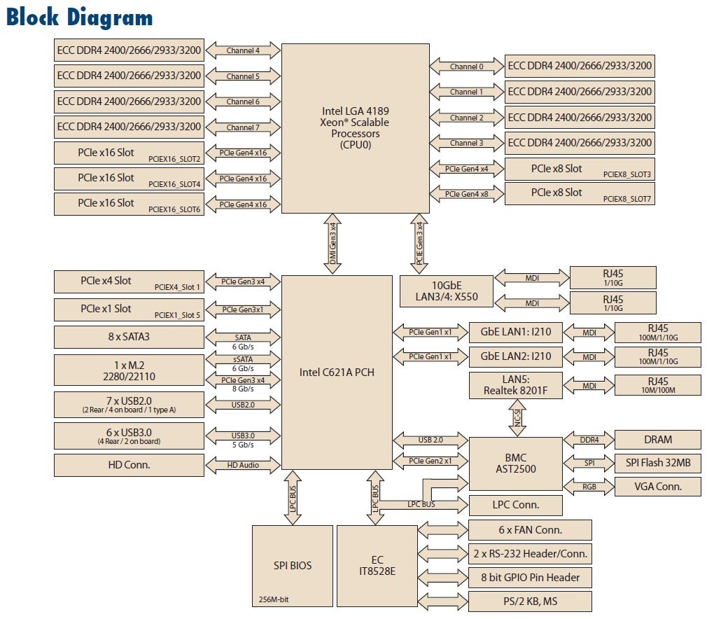
AWS Graviton3 CPU with 64 Cores and DDR5 Memory Available with Three Sockets Per Motherboard

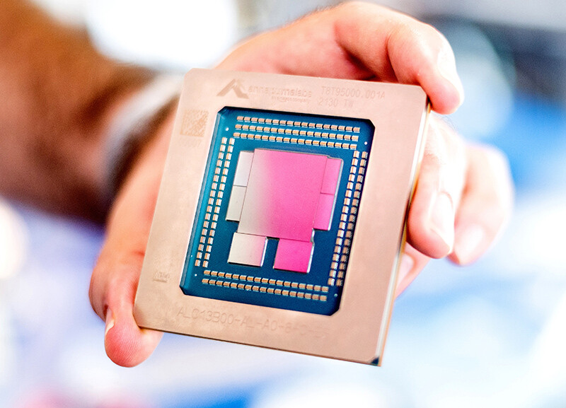
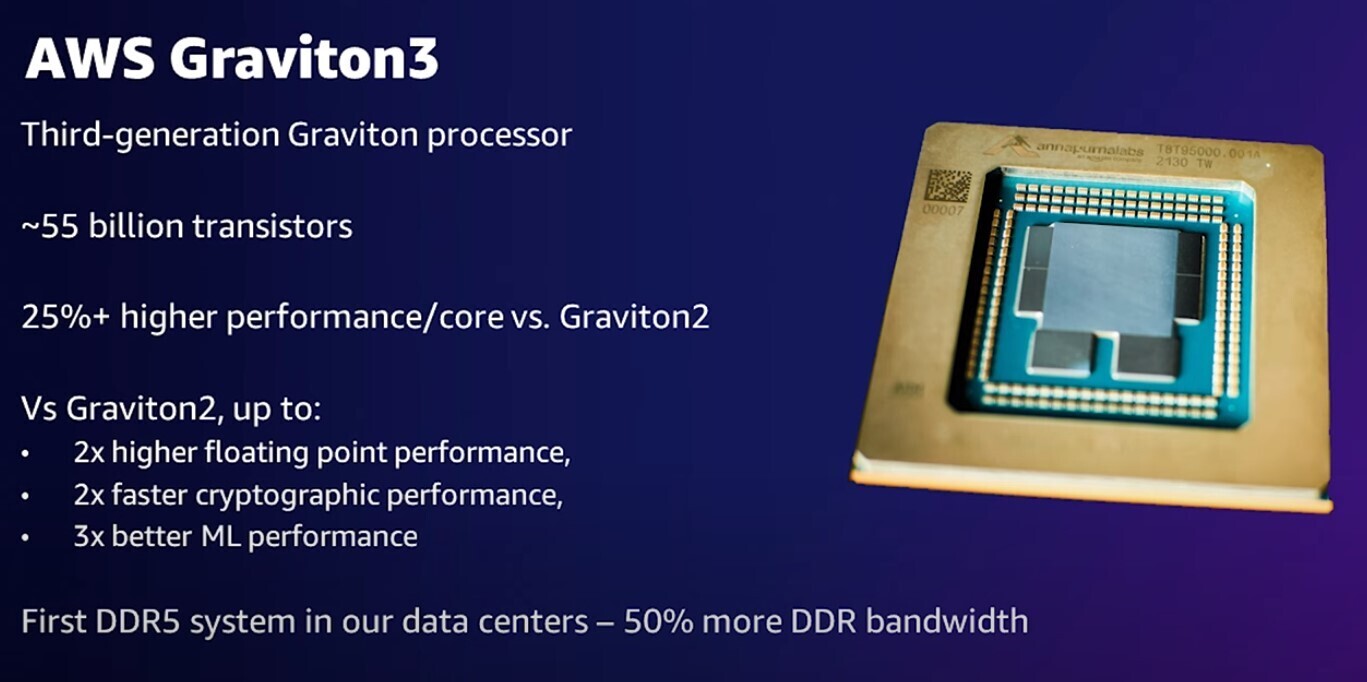
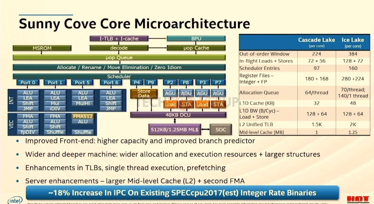
Amazon's AWS division has been making Graviton processors for a few years now, and the company recently announced its Graviton3 design will soon to available in the cloud. Today, we are witnessing a full launch of the Graviton3 CPUs with the first instances available in the AWS Cloud. In theC7g instances, AWS customers can now scale their workloads across 1-64 vCPU instance variants. Graviton3's 64 cores run at 2.6 GHz clock speed, 300 GB/sec maximum memory bandwidth, DDR5 memory controller, 64 cores, seven silicon die chiplet-based design, 256-bit SVE (Scalable Vector Extension), all across 55 billion transistors. Paired with up to 128 GiB of DDR5 memory, these processors are compute-intensive solutions. AWS noted that the company used a monolithic computing and memory controller logic design to reduce latency and improve performance.

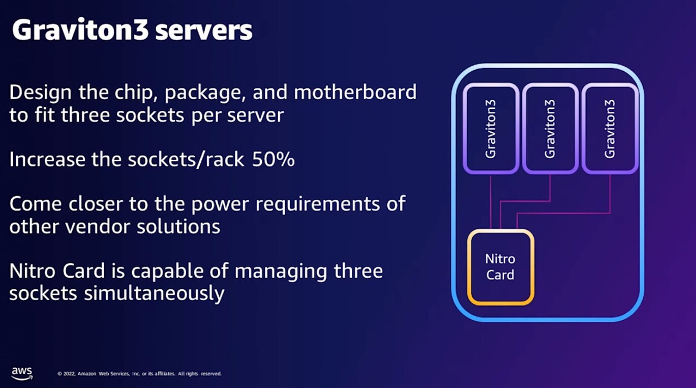
One interesting thing to note is the motherboard that AWS hosts Graviton3 processors in. Usually, server motherboards can be single, dual, or quad-socket solutions. However, AWS decided to implement a unique solution with three sockets. This tri-socket setup is designed to see each CPU as an independent processor, managed by a Nitro Card, which can handle exactly three CPUs. The company notes that the CPU is now in general availability with C7g instances and you can see it below.

Supermicro Accelerates AI Workloads, Cloud Gaming, Media Delivery with New Systems Supporting Intel's Arctic Sound-M and Intel Habana Labs Gaudi 2

Super Micro Computer, Inc. (Nasdaq: SMCI), a global leader in enterprise computing, storage, networking, and green computing technology, supports two new Intel-based accelerators for demanding cloud gaming, media delivery, AI and ML workloads, enabling customers to deploy the latest acceleration technology from Intel and Intel Habana. "Supermicro continues to work closely with Intel and Habana Labs to deliver a range of server solutions supporting Arctic Sound-M and Gaudi 2 that address the demanding needs of organizations that require highly efficient media delivery and AI training," said Charles Liang, president and CEO. "We continue to collaborate with leading technology suppliers to deliver application-optimized total system solutions for complex workloads while also increasing system performance."

Supermicro can quickly bring to market new technologies by using a Building Block Solutions approach to designing new systems. This methodology allows new GPUs and acceleration technology to be easily placed into existing designs or, when necessary, quickly adapt an existing design when needed for higher-performing components. "Supermicro helps deliver advanced AI and media processing with systems that leverage our latest Gaudi 2 and Arctic Sound-M accelerators," stated Sandra Rivera, executive vice president and general manager of the Datacenter and AI Group at Intel. "Supermicro's Gaudi AI Training Server will accelerate deep learning training in some of the fastest growing workloads in the datacenter."

Fujitsu Achieves Major Technical Milestone with World's Fastest 36 Qubit Quantum Simulator

Fujitsu has successfully developed the world's fastest quantum computer simulator capable of handling 36 qubit quantum circuits on a cluster system featuring Fujitsu's "FUJITSU Supercomputer PRIMEHPC FX 700" ("PRIMEHPC FX 700")(1), which is equipped with the same A64FX CPU that powers the world's fastest supercomputer, Fugaku.

The newly developed quantum simulator can execute the quantum simulator software "Qulacs"(3) in parallel at high speed, achieving approximately double the performance of other significant quantum simulators in 36 qubit quantum operations. Fujitsu's new quantum simulator will serve as an important bridge towards the development of quantum computing applications that are expected to be put to practical use in the years ahead.

Tanzanite Silicon Solutions Demonstrates Industry's First CXL Based Memory Expansion and Memory Pooling Products

Tanzanite Silicon Solutions Inc., the leader in the development of Compute Express Link (CXL) based products, is unveiling its architectural vision and product roadmap with an SoC mapped to FPGA Proof-Of-Concept vehicle demonstrating Memory Expansion and Memory Pooling, with multi-host CXL based connectivity. Explosive demand for memory and compute to meet the needs of emerging applications such as Artificial Intelligence (AI), Machine Learning (ML), blockchain technology, and the metaverse is outpacing monolithic systems. A disaggregated data center design with composable components for CPU, memory, storage, GPU, and XPU is needed to provide flexible and dynamic pooling of resources to meet the varying demands of heterogenous workloads in an optimal and efficient manner.

Tanzanite's visionary TanzanoidTZ architecture and purpose-built design of a "Smart Logic Interface Connector" (SLICTZ) SoC enables independent scaling and sharing of memory and compute in a pool with low latency within and across server racks. The Tanzanite solution provides a highly scalable architecture for exa-scale level memory capacity and compute acceleration, supporting multiple industry standard form-factors, ranging from E1.S, E3.S, memory expansion board, and memory appliance.

Intel "Sapphire Rapids" Xeon 4-tile MCM Annotated

Intel Xeon Scalable "Sapphire Rapids" is an upcoming enterprise processor with a CPU core count of up to 60. This core-count is achieved using four dies inter-connected using EMIB. Locuza, who leads social media with logic die annotation, posted one for "Sapphire Rapids," based on a high-resolution die-shot revealed by Intel in its ISSCC 2022 presentation.

Each of the four dies in "Sapphire Rapids" is a fully-fledged multi-core processor in its own right, complete with CPU cores, integrated northbridge, memory and PCIe interfaces, and other platform I/O. What brings four of these together is the use of five EMIB bridges per die. This allows CPU cores of a die to transparantly access the I/O and memory controlled any of the other dies transparently. Logically, "Sapphire Rapids" isn't unlike AMD "Naples," which uses IFOP (Infinity Fabric over package) to inter-connect four 8-core "Zeppelin" dies, but the effort here appears to be to minimize the latency arising from an on-package interconnect, toward a high-bandwidth, low-latency one that uses silicon bridges with high-density microscopic wiring between them (akin to an interposer).

Intel Powers Latest Amazon EC2 General Purpose Instances with 3rd Gen Intel Xeon Scalable Processors

Intel today announced AWS customers can access the latest 3rd Gen Intel Xeon Scalable processors via the new Amazon Elastic Compute Cloud (Amazon EC2) M6i instances. Optimized for high-performance, general-purpose compute, the latest Intel-powered Amazon EC2 instances provide customers increased flexibility and more choices when running their Intel-powered infrastructure within the AWS cloud. Today's news is a further continuation of Intel and AWS' close collaboration, giving customers scalable compute instances in the cloud for almost 15 years.

"Our latest 3rd Gen Intel Xeon Scalable processors are our highest performance data center CPU and provide AWS customers an excellent platform to run their most critical business applications. We look forward to continuing our long-term collaboration with AWS to deploy industry-leading technologies within AWS' cloud infrastructure." -Sandra Rivera, Intel executive vice president and general manager, Datacenter and AI Group.

Xiaomi Announces CyberDog Powered by NVIDIA Jetson NX and Intel RealSense D450

Xiaomi today took another bold step in the exploration of future technology with its new bio-inspired quadruped robot - CyberDog. The launch of CyberDog is the culmination of Xiaomi's engineering prowess, condensed into an open source robot companion that developers can build upon.

CyberDog is Xiaomi's first foray into quadruped robotics for the open source community and developers worldwide. Robotics enthusiasts interested in CyberDog can compete or co-create with other like-minded Xiaomi Fans, together propelling the development and potential of quadruped robots.

Intel Xeon "Sapphire Rapids" Processor Die Shot Leaks

Thanks to the information coming from Yuuki_Ans, a person which has been leaking information about Intel's upcoming 4th generation Xeon Scalable processors codenamed Sapphire Rapids, we have the first die shots of the Sapphire Rapids processor and its delidded internals to look at. After performing the delidding process and sanding down the metal layers of the dies, the leaker has been able to take a few pictures of the dies present on the processor. As the Sapphire Rapids processor uses multi-chip modules (MCM) approach to building CPUs, the design is supposed to provide better yields for Intel and give the 10 nm dies better usability if defects happen.

In the die shots, we see that there are four dies side by side, with each die featuring 15 cores. That would amount to 60 cores present in the system, however, not all of the 60 cores are enabled. The top SKU is supposed to feature 56 cores, meaning that there would be at least four cores disabled across the configuration. This gives Intel flexibility to deliver plenty of processors, whatever the yields look like. The leaked CPU is an early engineering sample design with a low frequency of 1.3 GHz, which should improve in the final design. Notably, as Sapphire Rapids has SKUs that use in-package HBM2E memory, we don't know if the die configuration will look different from the one pictured down below.

Intel's Upcoming Sapphire Rapids Server Processors to Feature up to 56 Cores with HBM Memory

Intel has just launched its Ice Lake-SP lineup of Xeon Scalable processors, featuring the new Sunny Cove CPU core design. Built on the 10 nm node, these processors represent Intel's first 10 nm shipping product designed for enterprise. However, there is another 10 nm product going to be released for enterprise users. Intel is already preparing the Sapphire Rapids generation of Xeon processors and today we get to see more details about it. Thanks to the anonymous tip that VideoCardz received, we have a bit more details like core count, memory configurations, and connectivity options. And Sapphire Rapids is shaping up to be a very competitive platform. Do note that the slide is a bit older, however, it contains useful information.

The lineup will top at 56 cores with 112 threads, where this processor will carry a TDP of 350 Watts, notably higher than its predecessors. Perhaps one of the most interesting notes from the slide is the department of memory. The new platform will make a debut of DDR5 standard and bring higher capacities with higher speeds. Along with the new protocol, the chiplet design of Sapphire Rapids will bring HBM2E memory to CPUs, with up to 64 GBs of it per socket/processor. The PCIe 5.0 standard will also be present with 80 lanes, accompanying four Intel UPI 2.0 links. Intel is also supposed to extend the x86_64 configuration here with AMX/TMUL extensions for better INT8 and BFloat16 processing.

Intel to Launch 3rd Gen Intel Xeon Scalable Portfolio on April 6

Intel today revealed that it will launch its 3rd Generation Xeon Scalable processor series at an online event titled "How Wonderful Gets Done 2021," on April 6, 2021. This will be one of the first major media events headed by Intel's new CEO, Pat Gelsinger. Besides the processor launch, Intel is expected to detail many of its advances in the enterprise space, particularly in the areas of 5G infrastructure rollout, edge computing, and AI/HPC. The 3rd Gen Xeon Scalable processors are based on the new 10 nm "Ice Lake-SP" silicon, heralding the company's first CPU core IPC gain in the server space since 2015. The processors also introduce new I/O capabilities, such as PCI-Express 4.0.

HPE Lists 40-Core Intel Ice Lake-SP Xeon Server Processor

Hewlett Packard Enterprise, the company focused on making enterprise hardware and software, has today mistakenly listed some of Intel's upcoming 3rd generation Xeon Scalable processors. Called Ice Lake-SP, the latest server processor generation is expected to launch sometime in the coming days, with a possible launch date being the March 23rd "Intel Unleashed" webcast. The next generation of processors will finally bring a new vector of technologies Intel needs in server space. That means the support for PCIe 4.0 protocol for higher speed I/O and octa-channel DDR4 memory controller for much greater bandwidth. The CPU lineup will for the first time use Intel's advanced 10 nm node called 10 nm SuperFin.

Today, in the leaked HPE listing, we get to see some of the Xeon models Intel plans to launch. Starting from 32-core models, all the way to 40-core models, all SKUs above 28 cores are supposed to use dual die configuration to achieve high core counts. The limit of a single die is 28 cores. HPE listed a few models, with the highest-end one being the Intel Xeon Platinum XCC 8380 processor. It features 40 cores with 80 threads and a running frequency of 2.3 GHz. If you are wondering about TDP, it looks like the 10 nm SuperFin process is giving good results, as the CPU is rated only for 270 Watts of power.

Intel Announces Its Next Generation Memory and Storage Products

Today, at Intel's Memory and Storage 2020 event, the company highlighted six new memory and storage products to help customers meet the challenges of digital transformation. Key to advancing innovation across memory and storage, Intel announced two new additions to its Intel Optane Solid State Drive (SSD) Series: the Intel Optane SSD P5800X, the world's fastest data center SSD, and the Intel Optane Memory H20 for client, which features performance and mainstream productivity for gaming and content creation. Optane helps meet the needs of modern computing by bringing the memory closer to the CPU. The company also revealed its intent to deliver its 3rd generation of Intel Optane persistent memory (code-named "Crow Pass") for cloud and enterprise customers.

"Today is a key moment for our memory and storage journey. With the release of these new Optane products, we continue our innovation, strengthen our memory and storage portfolio, and enable our customers to better navigate the complexity of digital transformation. Optane products and technologies are becoming a mainstream element of business compute. And as a part of Intel, these leadership products are advancing our long-term growth priorities, including AI, 5G networking and the intelligent, autonomous edge." -Alper Ilkbahar, Intel vice president in the Data Platforms Group and general manager of the Intel Optane Group.

Intel Introduces new Security Technologies for 3rd Generation Intel Xeon Scalable Platform, Code-named "Ice Lake"

Intel today unveiled the suite of new security features for the upcoming 3rd generation Intel Xeon Scalable platform, code-named "Ice Lake." Intel is doubling down on its Security First Pledge, bringing its pioneering and proven Intel Software Guard Extension (Intel SGX) to the full spectrum of Ice Lake platforms, along with new features that include Intel Total Memory Encryption (Intel TME), Intel Platform Firmware Resilience (Intel PFR) and new cryptographic accelerators to strengthen the platform and improve the overall confidentiality and integrity of data.

Data is a critical asset both in terms of the business value it may yield and the personal information that must be protected, so cybersecurity is a top concern. The security features in Ice Lake enable Intel's customers to develop solutions that help improve their security posture and reduce risks related to privacy and compliance, such as regulated data in financial services and healthcare.

Intel Enters Strategic Collaboration with Lightbits Labs

Intel Corp. and Lightbits Labs today announced an agreement to propel development of disaggregated storage solutions to solve the challenges of today's data center operators who are craving improved total-cost-of-ownership (TCO) due to stranded disk capacity and performance. This strategic partnership includes technical co-engineering, go-to-market collaboration and an Intel Capital investment in Lightbits Labs. Lightbits' LightOS product delivers high-performance shared storage across servers while providing high availability and read-and-write management designed to maximize the value of flash-based storage. LightOS, while being fully optimized for Intel hardware, provides customers with vastly improved storage efficiency and reduces underutilization while maintaining compatibility with existing infrastructure without compromising performance and simplicity.

Lightbits Labs will enhance its composable disaggregated software-defined storage solution, LightOS, for Intel technologies, creating an optimized software and hardware solution. The system will utilize Intel Optane persistent memory and Intel 3D NAND SSDs based on Intel QLC Technology, Intel Xeon Scalable processors with unique built-in artificial intelligence (AI) acceleration capabilities and Intel Ethernet 800 Series Network Adapters with Application Device Queues (ADQ) technology. Intel's leadership FPGAs for next-generation performance, flexibility and programmability will complement the solution.

Arm Announces Next-Generation Neoverse V1 and N2 Cores

Ten years ago, Arm set its sights on deploying its compute-efficient technology in the data center with a vision towards a changing landscape that would require a new approach to infrastructure compute.

That decade-long effort to lay the groundwork for a more efficient infrastructure was realized when we announced Arm Neoverse, a new compute platform that would deliver 30% year-over-year performance improvements through 2021. The unveiling of our first two platforms, Neoverse N1 and E1, was significant and important. Not only because Neoverse N1 shattered our performance target by nearly 2x to deliver 60% more performance when compared to Arm's Cortex-A72 CPU, but because we were beginning to see real demand for more choice and flexibility in this rapidly evolving space.

Intel Whitley Platform for Xeon "Ice Lake-SP" Processors Pictured

Here's is the first schematic of Intel's upcoming "Whitley" enterprise platform for the upcoming Xeon Scalable "Ice Lake-SP" processors, courtesy momomo_us. The platform sees the introduction of the new LGA4189 socket necessitated by Intel increasing the memory channels per socket to 8, compared to 6 of the current-gen "Cascade Lake-SP." The new platform also sees the introduction of PCI-Express gen 4.0 bus, with each socket putting out up to 64 PCI-Express gen 4.0 CPU-attached lanes. This are typically wired out as three x16 slots, two x8 slots, an x4 chipset bus, and a CPU-attached 10 GbE controller.

The processor supports up to 8 memory channels running at DDR4-3200 with ECC. The other key component of the platform is the Intel C621A PCH. The C621A talks to the "Ice Lake-SP" processor over a PCI-Express 3.0 x4 link, and appears to retain gen 3.0 fabric from the older generation C621. momomo_us also revealed that the 10 nm "Ice Lake-SP" processor could have TDP of up to 270 W.

Intel Xeon Scalable "Ice Lake-SP" 28-core Die Detailed at Hot Chips - 18% IPC Increase

Intel in the opening presentation of the Hot Chips 32 virtual conference detailed its next-generation Xeon Scalable "Ice Lake-SP" enterprise processor. Built on the company's 10 nm silicon fabrication process, "Ice Lake-SP" sees the first non-client and non-mobile deployment of the company's new "Sunny Cove" CPU core that introduces higher IPC than the "Skylake" core that's been powering Intel microarchitectures since 2015. While the "Sunny Cove" core itself is largely unchanged from its implementation in 10th Gen Core "Ice Lake-U" mobile processors, it conforms to the cache hierarchy and tile silicon topology of Intel's enterprise chips.

The "Ice Lake-SP" die Intel talked about in its Hot Chips 32 presentation had 28 cores. The "Sunny Cove" CPU core is configured with the same 48 KB L1D cache as its client-segment implementation, but a much larger 1280 KB (1.25 MB) dedicated L2 cache. The core also receives a second fused multiply/add (FMA-512) unit, which the client-segment implementation lacks. It also receives a handful new instruction sets exclusive to the enterprise segment, including AVX-512 VPMADD52, Vector-AES, Vector Carry-less Multiply, GFNI, SHA-NI, Vector POPCNT, Bit Shuffle, and Vector BMI. In one of the slides, Intel also detailed the performance uplifts from the new instructions compared to "Cascade Lake-SP".

Chenbro RB133G13-U10: Barebone 1U Dual Xeon NVMe SSD Server System

Chenbro launches the RB133G13-U10, a 1U dual Intel Xeon Scalable NVMe SSD server barebone system designed for all-flash array (AFA), tiered and virtualized storage applications in Enterprise. Offering Intel VROC, Apache Pass, and Redfish compliance, the RB133G13-U10 is ideal for high-performance applications such as software-defined storage, virtualization, HPC, Cloud computing, and SaaS, with end-to-end security and effortless management. The scale-up storage design helps Enterprise remain agile to meet future business needs.

The RB133G13-U10 is a custom 1U chassis pre-fitted with dual Intel Xeon motherboard. Ready to install two Intel Xeon Scalable processors with up to 28-cores, 165 W TDP, with a maximum of 2 TB of DDR4 memory, 2X 10 GbE connectivity, 1X PCI-E Gen 3 x16 HH/HL expansion slot and with support for up to 10X hot-swappable NVMe U.2 drives, it is an ideal barebone storage solution that scales as a company's needs grow.

GIGABYTE Launches R292 Servers Supporting 4-way 3rd Gen Intel Xeon Scalable Processors

GIGABYTE, an industry leader in high-performance servers and workstations, today announced the launch of the GIGABYTE R292 servers featuring four 3rd Gen Intel Xeon Scalable processors, supporting four double-slot accelerators in the R292-4S0, and eight full-height half-length expansion cards in the R292-4S1.

The R292 series server supports four 3rd Gen Intel Xeon Scalable processors. Each processor can perform data transfer or share workload at 20.8GT/s with the other three processors on the motherboard. Its breakthrough computing power can be used to power mission-critical application at scale and analyze growing data at extraordinary speeds.

Possible Intel "Ice Lake-SP" 24-core Xeon Processor Surfaces on Geekbench Database

Intel plans to update its Xeon Scalable server processor family this year with the new "Ice Lake-SP" microarchitecture. Built on the 10 nm+ silicon fabrication process, "Ice Lake-SP" is a high- thru extreme core-count monolithic silicon that features "Sunny Cove" CPU cores that introduce the first real IPC increases over "Skylake." A 24-core/48-thread processor likely based on this silicon surfaced on the Geekbench database, where it posted some impressive numbers given its low clock speeds.

The processor comes with an identification string "GenuineIntel Family 6 Model 106 Stepping 4," with a nominal clock speed of 2.20 GHz, and boost frequency of 2.90 GHz, which points to the possibility of this being an engineering sample. Besides clock speeds and core counts, some basic hardware specs were detected by Geekbench 4. For starters, the processor has an L1D cache size of 48 KB and L1I cache size of 32 KB, which is similar to the client-segment "Ice Lake-U" silicon based Core i7-1065G7, and confirms that this processor uses "Sunny Cove" cores. "Cascade Lake" and "Skylake" cores use 32 KB L1D caches. Also, the dedicated L2 cache per core is 1.25 MB, up from the 1 MB L2 caches on "Cascade Lake." Client-segment "Ice Lake" chips use 512 KB L2 caches. The shared L3 cache is 36 MB (or 1.5 MB slice per core), which loosely aligns with the cache balance of Intel's server and HEDT processors. In this bench run, the processor is backed by 256 GB of memory, of an unknown type or configuration. In the three bench runs, the setup scores roughly 4100 points single-core, and roughly 42000 points multi-core.

Intel Reports First-Quarter 2020 Financial Results

Intel Corporation today reported first-quarter 2020 financial results. "Our first-quarter performance is a testament to our team's focus on safeguarding employees, supporting our supply chain partners and delivering for our customers during this unprecedented challenge," said Bob Swan, Intel CEO."The role technology plays in the world is more essential now than it has ever been, and our opportunity to enrich lives and enable our customers' success has never been more vital. Guided by our cultural values, competitive advantages and financial strength, I am confident we will emerge from this situation an even stronger company."

In the first quarter, Intel achieved 34 percent data-centric revenue growth and 14 percent PC-centric revenue growth YoY. The company maintained essential factory operations with greater than 90 percent on-time delivery while supporting employees, customers and communities in response to the COVID-19 pandemic. This includes a new Intel Pandemic Response Technology Initiative to combat the virus where we can uniquely make a difference with Intel technology, expertise, and resources.

Intel Restarts 14 nm Operations in Costa Rica, Aims to Increase Capacity for Xeon Output

Intel has decided to restart operations in its previously winded-down Costa Rica facilities. An Intel Product Change Notification (PCN) for their Cascade Lake Xeon Scalable processors shows that the company has added Costa Rica to its three other "Test and Finish" sites - the other three are located in Penang (Malaysia), Kulim (Malaysia) and Vietnam. Intel's aim is to guarantee a "continuous supply" of the affected processors - namely, Cascade Lake second-generation Xeon Scalable processors in the Silver, Gold and Platinum lines (in both boxed and tray SKUs).

This move, which will be done in phases. The first implementation of the Costa Rica operations will be effective on April 19th, with the remaining operations to come online on August 3rd. Intel expects to reduce dependency on their other three Test and Finish sites, while being able to bolster final production capacity by some 25% with this move.

ASUS Announces Exclusive Power Balancer Technology and Servers with New 2nd Gen Intel Xeon Scalable

ASUS, the leading IT Company in server systems, server motherboards, workstations and workstation motherboards today announced exclusive Power Balancer technology to support the new 2nd Gen Intel Xeon Scalable Processor (extended Cascade Lake-SP refresh SKUs) across all server product lineups, including the RS720/720Q/700 E9, RS520/500 E9 and ESC8000/4000 G4 series server systems and Z11 server motherboards.

In complex applications, such as high-performance computing (HPC), AI or edge computing, balancing performance and power consumption is always a challenge. With Power Balancer technology and the new 2nd Gen Intel Xeon Scalable Processor, ASUS servers save up to 31 watts power per node on specific workloads and achieve even better efficiency with more servers in large-scale environments, significantly decreasing overall power consumption for a much lower total cost of ownership and optimized operations.

Intel Discontinues Omni-Path Enabled Xeon Processors

Intel's Omni-Path technology has been used primarily in high performance computing market, in order to provide high speed interconnect between Intel Xeon CPUs, with speeds reaching around 100 Gbps. Accompanied by different design and system integration that Omni-Path uses, it was a bit difficult to integrate into server system, while not adding much value that other technologies couldn't match or beat.

Because of these reasons, Intel is now discontinuing its last product capable of utilizing Omni-Path - the first generation Xeon Scalable CPUs. Carrying the suffix "F", these CPUs had an extra connector sticking out of CPU's PCB to enable the Omni-Path functionality (see images bellow). There were eight CPUs manufactured in total that had this extra feature, consisting out of two Xeon Platinum and six Xeon Gold CPUs, which have now reached end of life. Intel states that focus from these CPUs has shifted to other technologies like silicon photonics, which provides much greater speed reaching 100s of gigabits per second. Intel already demonstrated transceivers capable of reaching 400 Gb/s speeds with the magic of light, which will become available in 1H 2020.

LGA 4189 is the Latest Socket for Intel's Next Generation of Xeon CPUs

TE Connectivity, the maker of various kinds of connectivity solutions for computer systems, has released its latest iteration of the LGA socket for the next generation of Xeon Scalable CPUs. Being validated by Intel, the LGA 4189-4 and LGA 4189-5 are going to power the next generation of 10 nm Xeon CPUs, based on the Ice Lake architecture, and up to 56-core 2nd generation Xeon Scalable CPUs. While there are two models of the socket, TE Connectivity didn't reveal what the differences are between them. Socket P4 (LGA 4189-4) and P5 (LGA 4189-5) also feature exactly the same pin count, 0.9906 mm hex pitch and 2.7 mm SP height, so we can only speculate that the "4" or "5" in the revision is supposed to indicate details like higher power delivery capability or support for Ice Lake CPUs.

In addition to providing a new socket for Ice Lake, these sockets have support for PCI-Express Gen 4.0 and eight-channel memory (supported memory configurations are vendor dependent), meaning that we are getting two more memory channels than previous Xeon CPUs with a faster and newer PCIe standard.
Return to Keyword Browsing
May 21st, 2024 18:51 EDT change timezone

New Forum Posts

Popular Reviews

Controversial News Posts