News Posts matching #Semiconductor

Return to Keyword Browsing

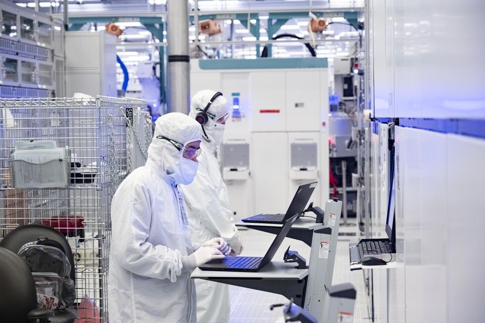
Kyocera to Build Its Largest Plant in Japan, Increasing Production of Semiconductor Components

Kyocera Corporation (hereinafter "Kyocera;" President: Hideo Tanimoto) today announced a plan to build the largest manufacturing facility it has ever operated in Japan, expanding production capacity for components including organic semiconductor packages and crystal device packages. A signing ceremony held April 20, 2022 was attended by Kagoshima Governor Koichi Shiota, Satsumasendai City Mayor Ryoji Tanaka, and Kyocera officials. Construction is scheduled to begin next month at the company's Sendai Plant Campus in Kagoshima.

Three converging factors are creating strong demand for Kyocera's organic semiconductor packages and crystal device packages. Smart vehicles are expanding the need for automotive cameras and high-performance processors used in Advanced Driver-Assistance Systems (ADAS) and autonomous driving. New communications infrastructures, including fifth-generation (5G) base stations and datacenters, are being deployed worldwide. In addition, the rising trend toward digitalization is expanding demand for electronic products ranging from personal computers and smartphones to consumer goods, industrial automation, and others. Kyocera will open the new facility in October 2023 to serve these growing trends, aiming for a 4.5-fold increase in production capacity for organic packages at the Sendai Plant Campus, as well as a substantial increase in capacity for crystal device packages. Kyocera will contribute to the community by stimulating economic development in Kagoshima, creating new employment opportunities through expanded production of semiconductor components in response to global demand.

Intel, Micron, and Analog Devices Join MITRE Engenuity's Semiconductor Alliance to Define Principles for Joint Research and Collaboration

Intel, Micron, Analog Devices, and MITRE Engenuity announced they have an agreement of principles to accelerate semiconductor research, development, and prototyping to build a more robust U.S. semiconductor industry, foster advanced manufacturing in the United States, and protect intellectual property amid increased global competition. This engagement signifies a commitment to collaborate on ensuring the resiliency of the industry. It establishes the Semiconductor Alliance to propose the foundation for a whole-of-nation approach for a more innovation-focused U.S. semiconductor industry and supply chain, one that ensures American innovation truly leads to American growth.

The Semiconductor Alliance, led by MITRE Engenuity, was developed from working groups in 2021, and its principles were published in a white paper on American Innovation for American Growth summarizing the Alliance's whole-of-nation call to action for a fair and objective National Semiconductor Technology Center (NSTC). The leading U.S. semiconductor manufacturers—Intel, Micron, and Analog Devices—and MITRE Engenuity seek engagement from industry and experts from all facets of the U.S. semiconductor ecosystem, including integrated device manufacturers; fabless chip companies; providers of infrastructure, design, and manufacturing tools; and technology innovators from industry and academia. MITRE Engenuity is built on MITRE's 60+ year history of serving as an independent, objective bridge and convener of government, industry, and academia, bringing together the whole of nation to tackle some of the biggest challenges to our national security.

ERS electronic unveils its third-generation flagship thermal debond machine

ERS electronic, the industry leader in the market of thermal management solutions for semiconductor manufacturing, reveals the details of its third-generation flagship thermal debond machine, ADM330. The machine was introduced to the market in 2007 as the first-of-its-kind. Since then, it has become an industry-favourite and can be found on the production floors of most semiconductor manufacturers and OSATs involved in Advanced Packaging worldwide.
Earlier this month, the company was recognized for its continuous innovation and contribution to heterogeneous integration technologies with a 3D InCites "Equipment Supplier of the Year" award.

ERS is now giving a first look at the next-generation ADM330, which has changed its previously matte metallic appearance to a clean, white surface matching most equipment found in a cleanroom. In addition, the machine is now fully compliant with the GEM300 SEMI standards, thus allowing seamless integration into automated fabs and Industry 4.0 architectures. Warpage adjustment performance has also been improved thanks to a unique thermal chuck design that enables a strong vacuum performance three times better than its predecessor. Lastly, the new ADM330 offers an implemented add-on software feature allowing stand-alone laser marking for improved wafer traceability.

Taiwan Rocked by 6.6 Earthquake, Causes no Serious Production Issues

At 01:41 in the morning of the 23rd of March, the southeast coast of Taiwan experienced a magnitude 6.6 earthquake in the ocean outside Hualien County. The quake was felt island wide and some of the factories that operate 24/7 evacuated staff as a precautionary measure. All affected companies claim to have resumed operations later the same day, after checking that no damage was caused by the quake. The southeast of Taiwan kept being hit by minor quakes for the rest of the night and day, with some being felt across the island.

TSMC and UMC both claimed that the quake had a minimal effect on production, although production equipment had gone into self-protect mode, which was largely the reason for no production issues taking place. Powerchip Semiconductor on the other hand had a two to three hour production loss and Vanguard International Semiconductor was reported saying they were checking for defects in their production. AU Optronics and Innolux were also saved by their various safeguards against earthquake damage and both companies were expecting to return to normal production shortly. Other companies are said to have reported issues with their production equipment, but no damage to the actual products they produce.

ASML is the Next Bottle Neck in Chip Manufacturing

There have been several announcements of new semiconductor fabs being built all over the world, but those fabs might end up being empty shells, all because of a single company. ASML or Advanced Semiconductor Materials Lithography if you prefer, is a Dutch company that produces various types of photolithography machines that are used to produce semiconductors. They're the world leader in their field and their machines are used by the likes of Intel and TSMC to do the physical etching of the silicon wafers that semiconductors are produced from. Now a warning from ASML's CEO, Peter Wennink has arrived, stating that the company can't keep up with demand.

The company isn't expecting to fulfil orders for at least the next couple of years, despite expecting to ship more machines this year than last year and more machines next year than this year. As each of these machines are largely custom made for its customers and hand built, due to the low production volumes, it takes a lot of time to construct each of these huge machines. Wennink said that the company "really needs to step up our capacity significantly more than 50 per cent. That will take time."

Top 10 Foundries Post Record 4Q21 Performance for 10th Consecutive Quarter at US$29.55B, Says TrendForce

The output value of the world's top 10 foundries in 4Q21 reached US$29.55 billion, or 8.3% growth QoQ, according to TrendForce's research. This is due to the interaction of two major factors. One is limited growth in overall production capacity. At present, the shortage of certain components for TVs and laptops has eased but there are other peripheral materials derived from mature process such as PMIC, Wi-Fi, and MCU that are still in short supply, precipitating continued fully loaded foundry capacity. Second is rising average selling price (ASP). In the fourth quarter, more expensive wafers were produced in succession led by TSMC and foundries continued to adjust their product mix to increase ASP. In terms of changes in this quarter's top 10 ranking, Nexchip overtook incumbent DB Hitek to clinch 10th place.

TrendForce believes that the output value of the world's top ten foundries will maintain a growth trend in 1Q22 but appreciation in ASP will still be the primary driver of said growth. However, since there are fewer first quarter working days in the Greater China Area due to the Lunar New Year holiday and this is the time when some foundries schedule an annual maintenance period, 1Q22 growth rate will be down slightly compared to 4Q21.

8-inch Substrate Mass Production in 2H22, 3rd Gen Power Semiconductor CAGR to Reach 48% by 2025, Says TrendForce

At present, the materials with the most development potential are Wide Band Gap (WBG) semiconductors with high power and high frequency characteristics, including silicon carbide (SiC) and gallium nitride (GaN), which are mainly used in electric vehicles (EV) and the fast charging battery market. TrendForce research estimates, the output value of third generation power semiconductors will grow from US$980 million in 2021 to US$4.71 billion in 2025, with a CAGR of 48%.

SiC is suitable for high-power applications, such as energy storage, wind power, solar energy, EVs, new energy vehicles (NEV) and other industries that utilize highly demanding battery systems. Among these industries, EVs have attracted a great deal of attention from the market. However, most of the power semiconductors used in EVs currently on the market are Si base materials, such as Si IGBT and Si MOSFET. However, as EV battery power systems gradually develop to voltage levels greater than 800 V, compared with Si, SiC will produce better performance in high-voltage systems. SiC is expected to gradually replace part of the Si base design, greatly improve vehicle performance, and optimize vehicle architecture. The SiC power semiconductor market is estimated to reach US$3.39 billion by 2025.

Canada is the Next Nation That is Getting Ready to Invest in the Semiconductor Industry

The Canadian government is getting ready to invest C$240 million (about US$187 million) into what the country calls the Semiconductor Challenge Callout. C$90 million of that will go towards the Canadian Photonics Fabrication Centre (CPFC), which is as the name implies, a facility that engineers and manufactures a range of photonics products, mostly on the prototyping level. The remaining C$150 million is up for grabs through the Strategic Innovation Fund, which is a government fund set up to help Canadian companies grow.

François-Philippe Champagne, the Canadian Minister of Innovation, Science and Industry is quoted as saying "By investing in Canada's semiconductor industry, we are making a firm commitment to businesses looking to invest in Canada. Whether it's high-value or large-scale manufacturing, we want to see Canada be home to the world's leading semiconductor manufacturers.". Exactly which companies will be asking for a share of the money is currently up in the air, but according to The Register, the Canadian government is looking for a wide range of potential semiconductor related businesses. Some examples are 2.5D and 3D chip packaging, MEMS sensor manufacturing and so on. None of this is compared to what the US, EU, Taiwan, Korea and the PRC are currently working on, but it could very well end up being supplemental to much of what's going on in the US semiconductor market right now.

Intel, AMD, Arm, and Others, Collaborate on UCIe (Universal Chiplet Interconnect Express)

Intel, along with Advanced Semiconductor Engineering Inc. (ASE), AMD, Arm, Google Cloud, Meta, Microsoft Corp., Qualcomm Inc., Samsung and Taiwan Semiconductor Manufacturing Co., have announced the establishment of an industry consortium to promote an open die-to-die interconnect standard called Universal Chiplet Interconnect Express (UCIe). Building on its work on the open Advanced Interface Bus (AIB), Intel developed the UCIe standard and donated it to the group of founding members as an open specification that defines the interconnect between chiplets within a package, enabling an open chiplet ecosystem and ubiquitous interconnect at the package level.

"Integrating multiple chiplets in a package to deliver product innovation across market segments is the future of the semiconductor industry and a pillar of Intel's IDM 2.0 strategy," said Sandra Rivera, executive vice president and general manager of the Datacenter and Artificial Intelligence Group at Intel. "Critical to this future is an open chiplet ecosystem with key industry partners working together under the UCIe Consortium toward a common goal of transforming the way the industry delivers new products and continues to deliver on the promise of Moore's Law."

Semiconductor Makers Don't Expect Russia-Ukraine War to Worsen Chip Shortages

Much of the globalized world's logistics is still in disarray from the COVID-19 pandemic, and now, Russia has thrown its weight on the matter through its invasion of Ukraine. As the initial offensive played out in the early hours of February 24th, semiconductor industry analysts turned to the situation with a prying eye - how exactly could this deadlock, and the following political and economical sanctions towards Russia, impact the semiconductor industry? The consensus seems to be a favorable one: not that much.

"The semiconductor industry has a diverse set of suppliers of key materials and gases, so we do not believe there are immediate supply disruption risks related to Russia and Ukraine," said John Neuffer, chief executive and president of the Semiconductor Industry Association. That sentiment was echoed by Intel; a company representative told Bloomberg that the company does not anticipate "(...) any impact on our supply chain. Our strategy of having a diverse, global supply chain minimizes our risk of potential local interruptions."

Intel Considering Semiconductor Fab in India

Back in December, we reported that Tower Semiconductor was one of several semiconductor manufacturers that was considering building a fab in India, largely due to government subsidies. Since then, Intel has stepped in and bought Tower Semiconductor and has taken over the negotiations with the Indian government. What has also come to light is that Tower Semiconductor has been in discussions with the Indian government for over a decade, but apparently the two parties have been unable to come up with a suitable agreement. Tower Semiconductor was apparently ready to cancel any plans on building in India as late as September 2021, but the more recent government initiative renewed their interest.

As to exactly what kind of fab Intel would build, is unclear at this point in time, but it might still be a MEMS fab or it could simply be a testing and packaging plant. Regardless of what kind of facility it'll be, it's interesting that Intel decided to keep the ongoing plans from Tower Semiconductor going. Tower Semiconductor mostly manufactured for fabless companies and were producing some two million wafers a year. It's likely that Intel will carry on producing for the same companies at the same terms for now, although as Tower Semiconductor gets integrated closer with the Intel foundry, things could change.

Intel Reportedly Acquiring Tower Semiconductor for $6 Billion

Update: The Intel acquisition of Tower Semiconductor has gone through for a value of $5.4 billion, at a price of $53 per share. Through the deal, Intel adds Tower Semiconductor's infrastructure, IP, technicians, logistics and clients to its portfolio. Intel CEO Pat Gelsinger said that "Tower's specialty technology portfolio, geographic reach, deep customer relationships and services-first operations will help scale Intel's foundry services and advance our goal of becoming a major provider of foundry capacity globally." He then added that "This deal will enable Intel to offer a compelling breadth of leading-edge nodes and differentiated specialty technologies on mature nodes - unlocking new opportunities for existing and future customers in an era of unprecedented demand for semiconductors." The original story follows.

Intel is reportedly looking to increase its manufacturing capability - and its cadre of wafer-purchasing clients - by acquiring Israeli semiconductor manufacturer Tower Semiconductor. If true, the deal will bring seven additional foundries to Intel's existing infrastructure, capable of 2 million wafer starts per year. The foundries are located across three continents: Tower Semiconductor owns and operates a 150 mm and a 200 mm fab in Migdal Haemek, Israel; two 200 mm fabs in the United States (Newport Beach, California and San Antonio, Texas); two 200 mm fabs in Japan; and one additional 300 mm fab in Japan. The deal could be finalized as soon as this week.

The EU Commission Proposes Chips Act to Confront Semiconductor Shortages and Strengthen Europe's Technological Leadership

Today, the Commission proposes a comprehensive set of measures to ensure the EU's security of supply, resilience and technological leadership in semiconductor technologies and applications. The European Chips Act will bolster Europe's competitiveness, resilience and help achieve both the digital and green transition. Recent global semiconductors shortages forced factory closures in a wide range of sectors from cars to healthcare devices. In the car sector, for example, production in some Member States decreased by one third in 2021. This made more evident the extreme global dependency of the semiconductor value chain on a very limited number of actors in a complex geopolitical context. But it also illustrated the importance of semiconductors for the entire European industry and society.

The EU Chips Act will build on Europe's strengths - world-leading research and technology organisations and networks as well as host of pioneering equipment manufacturers - and address outstanding weaknesses. It will bring about a thriving semiconductor sector from research to production and a resilient supply chain. It will mobilise more than €43 billion euros of public and private investments and set measures to prevent, prepare, anticipate and swiftly respond to any future supply chains disruption, together with Member States and our international partners. It will enable the EU to reach its ambition to double its current market share to 20% in 2030.

8-inch Wafer Capacity Remains Tight, Shortages Expected to Ease in 2H23, Says TrendForce

From 2020 to 2025, the compound annual growth rate (CAGR) of 12-inch equivalent wafer capacity at the world's top ten foundries will be approximately 10% with the majority of these companies focusing on 12-inch capacity expansion, which will see a CAGR of approximately 13.2%, according to TrendForce's research. In terms of 8-inch wafers, due to factors such as difficult to obtain equipment and whether capacity expansion is cost-effective, most fabs can only expand production slightly by means of capacity optimization, equating to a CAGR of only 3.3%. In terms of demand, the products primarily derived from 8-inch wafers, PMIC and Power Discrete, are driven by demand for electric vehicles, 5G smartphones, and servers. Stocking momentum has not fallen off, resulting in a serious shortage of 8-inch wafer production capacity that has festered since 2H19. Therefore, in order to mitigate competition for 8-inch capacity, a trend of shifting certain products to 12-inch production has gradually emerged. However, if shortages in overall 8-inch capacity is to be effectively alleviated, it is still necessary to wait for a large number of mainstream products to migrate to 12-inch production. The timeframe for this migration is estimated to be close to 2H23 into 2024.

Tachyum Selected for Pan-European Project Enabling 1 AI Zettaflop in 2024

Tachyum today announced that it was selected by the Slovak Republic to participate in the latest submission for the Important Projects of Common European Interest (IPCEI), to develop Prodigy 2 for HPC/AI. Prodigy 2 for HPC/AI will enable 1 AI Zettaflop and more than 10 DP Exaflops computers to support superhuman brain-scale computing by 2024 for under €1B. As part of this selection, Tachyum could receive a 49 million Euro grant to accelerate a second-generation of its Tachyum Prodigy processor for HPC/AI in a 3-nanometer process.

The IPCEI program can make a very important contribution to sustainable economic growth, jobs, competitiveness and resilience for industry and the economy in the European Union. IPCEI will strengthen the EU's open strategic autonomy by enabling breakthrough innovation and infrastructure projects through cross-border cooperation and with positive spill-over effects on the internal market and society as a whole.

Gartner: Worldwide Semiconductor Revenue Grew 25.1% in 2021, Exceeding $500 Billion For the First Time

Worldwide semiconductor revenue increased 25.1% in 2021 to total $583.5 billion, crossing the $500 billion threshold for the first time, according to preliminary results by Gartner, Inc.

"As the global economy bounced back in 2021, shortages appeared throughout the semiconductor supply chain, particularly in the automotive industry," said Andrew Norwood, research vice president at Gartner. "The resulting combination of strong demand as well as logistics and raw material price increases drove semiconductors' average selling price higher (ASP), contributing to overall revenue growth in 2021.

MediaTek Shows The World's First Live Demos of Wi-Fi 7 Technology to Customers and Industry Leaders

MediaTek today announced the world's first live demo of Wi-Fi 7 technology, highlighting the capabilities of its forthcoming Wi-Fi 7 Filogic connectivity portfolio. MediaTek is currently showcasing two Wi-Fi 7 demos to key customers and industry collaborators to demonstrate the technology's super-fast speeds and low latency transmission.

"The rollout of Wi-Fi 7 will mark the first time that Wi-Fi can be a true wireline/Ethernet replacement for super high-bandwidth applications," said Alan Hsu, corporate vice president and general manager of the Intelligent Connectivity business at MediaTek. "MediaTek's Wi-Fi 7 technology will be the backbone of home, office and industrial networks and provide seamless connectivity for everything from multi-player AR/VR applications to cloud gaming and 4K calls to 8K streaming and beyond."

Taiwan Aims to Become Self-sufficient in Semiconductor Equipment

The Taiwanese President, Tsai Ing-Wen, told local media that she believes that Taiwan can become self-sufficient when it comes to semiconductor equipment, although this is obviously not something that would happen overnight. A large part of why this has even been considered seems to be the current pandemic, as although Taiwan might not have suffered much from the pandemic itself, the nation has suffered when it comes to imports, as just in time production and delivery systems have broken down, which has affected most industries in Taiwan.

In 2021 Taiwanese semiconductor companies invested some NT$1 trillion (~US$36.3 billion), of which 70 percent was in equipment, according to the President, with around NT$600 billion (~US$21.8 billion) of that money being towards imported equipment. It also shows that local semiconductor equipment makers have a lot of work to do, especially if they're intending to catch up with their international competitors. The President also mentioned that the local semiconductor equipment industry grew by 28.7 percent in 2021, although it was still relatively small at NT$116.7 billion (~US$4.2 billion), but she was quoted as saying that she's 100 percent certain that Taiwan has the ability to make all semiconductor equipment the [local] industry needs.

ASML, Makers of Semiconductor Fab Machinery, Reports a Fire Incident

ASML, the company that makes semiconductor fab machinery that powers most of today's cutting-edge foundries, has reported a fire incident in one of its plants near Berlin. The company reports that the incident occurred at night, none of its employees are injured, and that the fire is extinguished. The company says that it does not know at this point how the incident affects supplies, since it hasn't undertaken a damage-assessment. The Berlin plant of ASML manufactures components of silicon lithography equipment, including some key mechanical and optical components, such as wafer tables and clamps, reticle chucks and mirror blocks. ASML inherited this plant when it acquired Berliner Glas in 2020.

Sony Develops World's First Stacked CMOS Image Sensor Technology with 2-Layer Transistor Pixel

Sony Semiconductor Solutions Corporation has succeeded in developing the world's first stacked CMOS image sensor technology with 2-Layer Transistor Pixel. Whereas conventional CMOS image sensors' photodiodes and pixel transistors occupy the same substrate, Sony's new technology separates photodiodes and pixel transistors on different substrate layers. This new architecture approximately doubles saturation signal level relative to conventional image sensors, widens dynamic range and reduces noise, thereby substantially improving imaging properties. The new technology's pixel structure will enable pixels to maintain or improve their existing properties at not only current but also smaller pixel sizes.

A stacked CMOS image sensor adopts a stacked structure consisting of a pixel chip made up of back-illuminated pixels stacked atop a logic chip where signal processing circuits are formed. Within the pixel chip, photodiodes for converting light to electrical signals, and pixel transistors for controlling the signals are situated alongside each other on the same layer. Increasing saturation signal level within form-factor constraints plays an important role in realizing high image quality with wide dynamic range.

India Next in Line With Incentives for Chip Makers

Over the past couple of months there have been a lot of calls for more investment into the semiconductor industry due to the current shortage of many different kinds of semiconductors. As we've seen, several government organizations have already started working on how to woo chip makers to their part of the world and the latest nation to join the fray is India.

Unlike the US and the EU where so far no firm budgets have been approved, India has already approved a US$10 billion incentive plan for semiconductor, as well as display panel manufacturers who are willing to consider India as the next location for their new fabs. According to Reuters, the Indian government is said to cover up to 50 percent of the project cost of new semiconductor and display panel fabs. So far it seems like at least three companies are interested in the scheme for semiconductor manufacturing, namely Tower Semiconductor out of Israel, Foxconn and an unnamed Singaporean consortium.

2021 Annual Global Power Management IC Prices Jump 10%, Supply Remains Tight for 1H22, Says TrendForce

Due to material shortages caused by insufficient semiconductor supply, to date, power management IC (PMIC) prices remain on an upward trend, according to TrendForce's latest investigations. Average selling price (ASP) for 1H22 is forecast to increase by nearly 10%, reaching a record six year high.

In terms of the global supply chain, in addition to the production capacity of major IDM manufacturers including TI, Infineon, ADI, STMicroelectronics, NXP, ON Semiconductor, Renesas, Microchip, ROHM (Maxim has been acquired by ADI and Dialog by Renesas), IC design houses such as Qualcomm and MediaTek (MTK) have obtained a certain level of production capacity from foundries. Of these, TI is in a leadership position and the aforementioned companies possess a combined market share of over 80%.

FTC Sues to Block $40 Billion Semiconductor NVIDIA and Arm Chip Merger

The Federal Trade Commission today sued to block U.S. chip supplier Nvidia Corp.'s $40 billion acquisition of U.K. chip design provider Arm Ltd. Semiconductor chips power the computers and technologies that are essential to our modern economy and society. The proposed vertical deal would give one of the largest chip companies control over the computing technology and designs that rival firms rely on to develop their own competing chips. The FTC's complaint alleges that the combined firm would have the means and incentive to stifle innovative next-generation technologies, including those used to run datacenters and driver-assistance systems in cars.

"The FTC is suing to block the largest semiconductor chip merger in history to prevent a chip conglomerate from stifling the innovation pipeline for next-generation technologies," said FTC Bureau of Competition Director Holly Vedova. "Tomorrow's technologies depend on preserving today's competitive, cutting-edge chip markets. This proposed deal would distort Arm's incentives in chip markets and allow the combined firm to unfairly undermine Nvidia's rivals. The FTC's lawsuit should send a strong signal that we will act aggressively to protect our critical infrastructure markets from illegal vertical mergers that have far-reaching and damaging effects on future innovations."

Samsung Electronics Announces New Advanced Semiconductor Fab Site in Taylor, Texas

Samsung Electronics, a world leader in advanced semiconductor technology, today announced that it would build a new semiconductor manufacturing facility in Taylor, Texas. The estimated $17 billion investment in the United States will help boost production of advanced logic semiconductor solutions that power next-generation innovations and technologies.

The new facility will manufacture products based on advanced process technologies for application in areas such as mobile, 5G, high-performance computing (HPC) and artificial intelligence (AI). Samsung remains committed to supporting customers globally by making advanced semiconductor fabrication more accessible and meeting surging demand for leading-edge products.

Fujitsu Launches New 8Mbit FRAM Guaranteeing Writing Endurance up to 100 Trillion Times

Fujitsu Semiconductor Memory Solution Limited has launched new 8 Mbit FRAM MB85R8M2TA with parallel interface, which is the first product to guarantee 100 trillion read/write cycle times in Fujitsu's FRAM product family. Evaluation samples are currently available. The new product achieves both high-speed operations, approximately 30% faster access speed, and low power consumption, 10% less operating current, compared to Fujitsu's conventional products. This memory IC is an ideal replacement of SRAM in the industrial machines that require high-speed operation.

FRAM is a non-volatile memory product with superior features of high read/write endurance, fast writing speed operation and low power consumption, and it has been mass-produced for over 20 years. Fujitsu has been providing 8 Mbit FRAM MB85R8M2T with parallel interface since June 2018. While promoting the product, the company heard voices of customer requirements such as guaranteed writing endurance of more than 10 trillion times, operation as fast as SRAM and TSOP package compatibility to SRAM. Fujitsu is now pleased to introduce its new 8 Mbit FRAM product satisfying these requirements, maintaining FRAM's unique feature of lower power consumption.
Return to Keyword Browsing
May 21st, 2024 18:11 EDT change timezone

New Forum Posts

Popular Reviews

Controversial News Posts