News Posts matching #Semiconductor

Return to Keyword Browsing

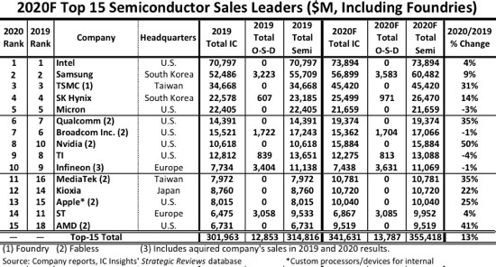
TSMC Could Build Six GigaFabs in Arizona

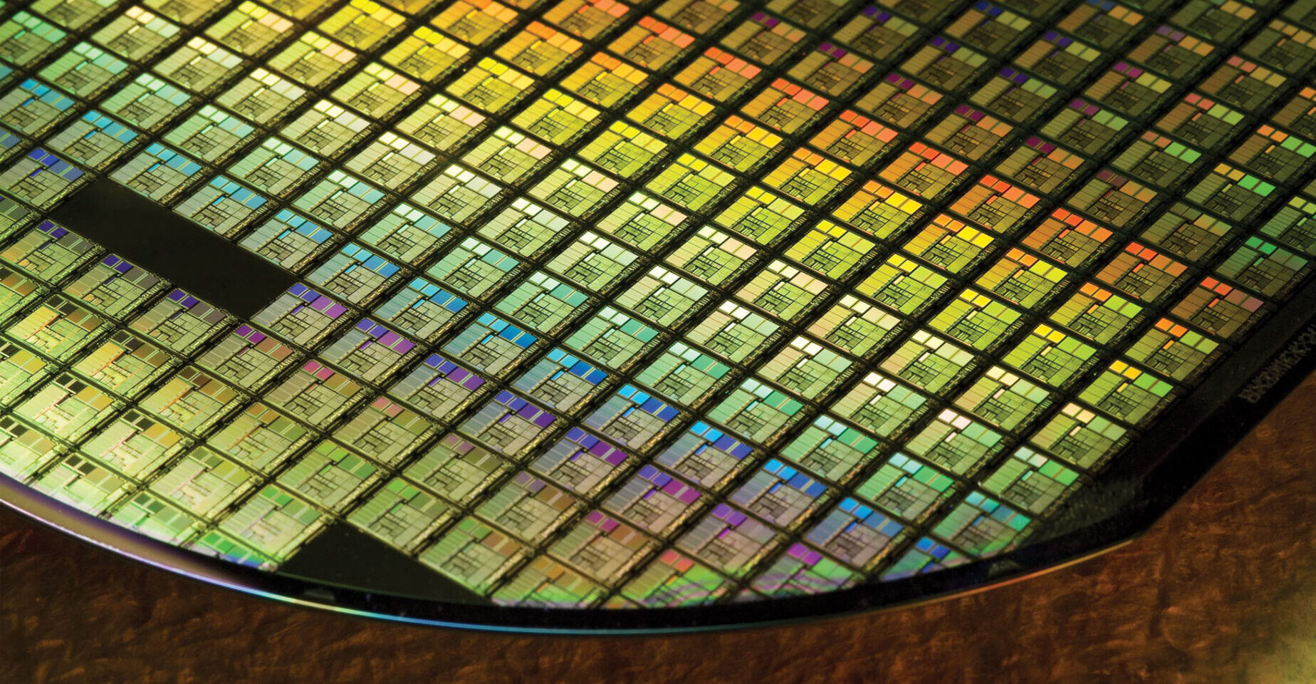
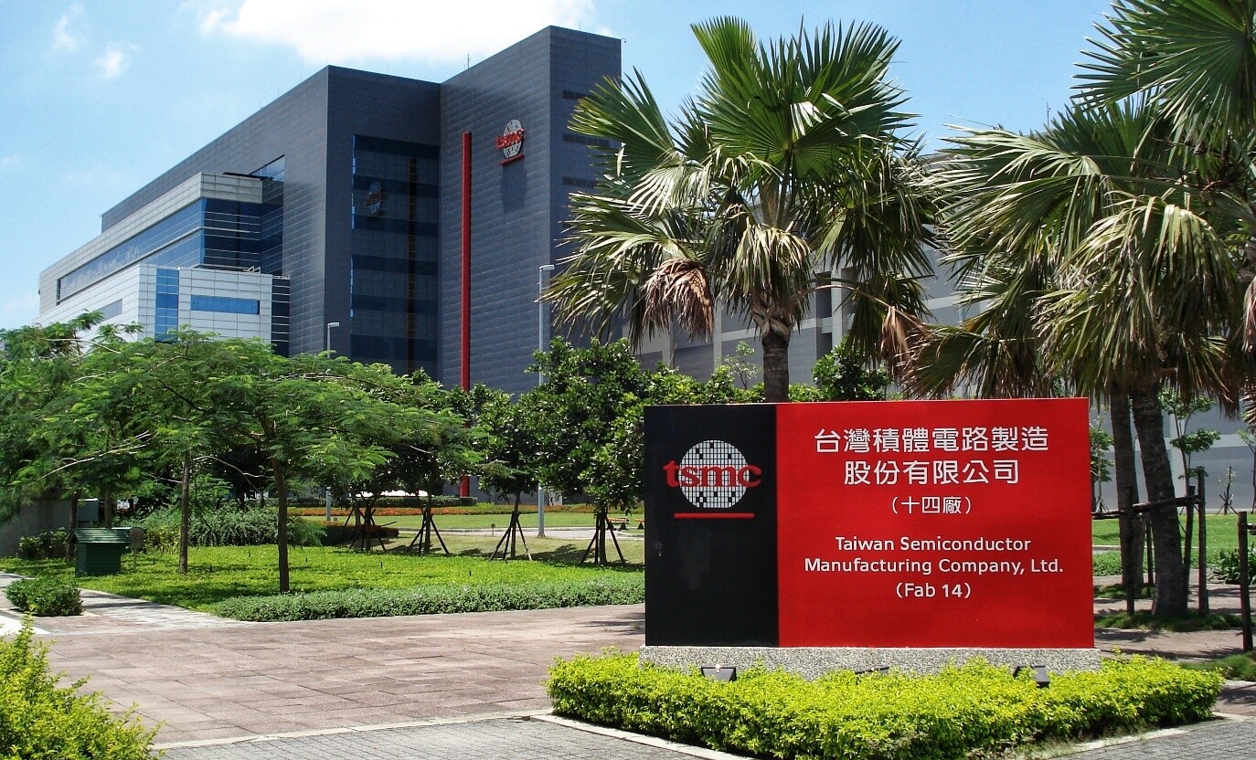
Taiwan Semiconductor Manufacturing Company (TSMC), one of the largest manufacturers of silicon, is seemingly making plans to build as many as six of its US-based fabs in Arizona. According to the unconfirmed report coming from UDN, TSMC could be building its Arizona-based factories for much larger capacities. Based on TSMC's classifications, the MegaFab-class of factories is the one with 25,000 WSPM output. According to the report, TSMC plans to build six additional facilities in the area where the Arizona fab is, and have a GigaFab-class (even larger type) factory present on US soil. Currently, the company operates six GigaFabs and all of them are based in Taiwan.

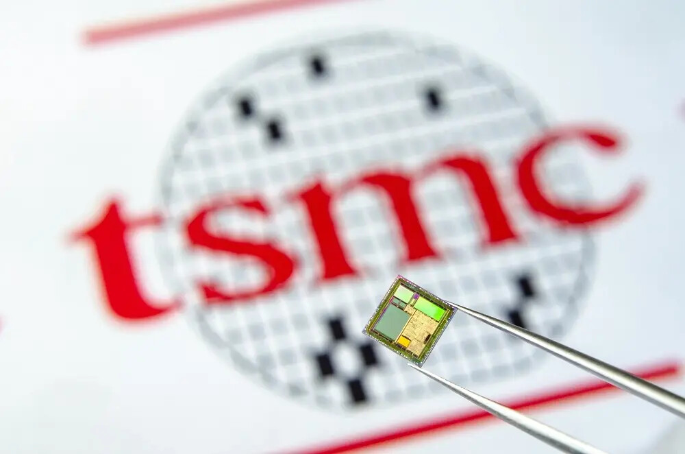
The GigaFab class factory is supposed to have over 100,000 WSPM output, and by building one in the US, TSMC could get much closer to big customers like Apple, NVIDIA, and AMD. Reports are saying that TSMC's primary target is 3 nm node production on 12-inch (300 mm) wafers. All six of the supposed facilities are expected to output more than 100,000 wafers at their peak, making it one of the largest projects TSMC has ever done. The Arizona location is supposed to serve as a "mega fab" facility and it is supposed to start manufacturing silicon in 2024. This information is, of course, just a rumor so you should take it with a grain of salt, as this type of information is usually only known by top-level management.

TSMC to Start 3 nm Node Production This Year

Taiwan Semiconductor Manufacturing Company (TSMC), the leading provider of semiconductors, is supposed to start 3 nm node production this year. While Samsung, one of the top three leading semiconductor foundries, has been struggling with the pandemic and delayed its 3 nm node for 2022, TSMC has managed to deliver it this year. According to a report, the Taiwanese semiconductor giant is preparing the 3 nm node for the second half of this year, with the correct date of high-volume product unknown. The expected wafer capacity for the new node is supposed to be around 30,000 wafers per month, with capacity expansion expected to hit around 105,000 wafers per month in 2023. This is similar to 5 nm's current numbers of 105,000 wafers per month output, which was 90,000 just a few months ago in Q4 2020. One of the biggest customers of the upcoming 3 nm node is Apple.

Report: TSMC and UMC are Trucking in Water Amid Shortages

Manufacturing silicon is no easy task. You need to have all the right supplies available all the time. One of the most used ingredients in silicon manufacturing is water. Almost every process needs it and it needs to be constantly available to the manufacturer. According to the report coming from Reuters, Taiwan Semiconductor Manufacturing Company (TSMC) and United Microelectronics Corporation (UMC) are experiencing water shortages. The Taiwan island is in trouble, as the typhoon season has been rather mild and water supplies are at the historic lows. Water restrictions are in place all across the island and the reservoirs in the center and southern regions are at only 20% capacity.

The lack of water is a big problem for TSMC and UMC, as both companies rely on the constant income of it. With water restrictions in place, TSMC has to keep its facilities running and needs to solve the problem. That is why Taiwan's biggest silicon manufacturer is now making small orders of waters, delivered by a truckload. TSMC expects to compensate for the lack of water coming from its regular sources with truckloads of it. While we do not know the numbers of it, we can expect the water use to be very high if we take into account the number of wafers TSMC produces at its facilities.

Industry Specialists Expect Chip Shortages to Last Until 2022

Industry specialists with various analysis groups have stated that they expect the world's current chip supply shortages to not only fail to be mitigated in the first half of 2021, but that they might actually last well into 2022. It's not just a matter of existing chip supply being diverted by scalpers, miners, or other secondary-market funnels; it's a matter of fundamental lack of resources and production capacity to meet demand throughout various quadrants of the semiconductor industry. With the increased demand due to COVID-19 and the overall increasingly complex design of modern chips - and increased abundance of individual chips within the same products - foundries aren't being able to scale their capacity to meet growing demand.

As we know, the timeframe between start and finish of a given semiconductor chip can sometimes take months. And foundries have had to extend their lead times (the time between a client placing an order and that order being fulfilled) already. This happens as a way to better plan out their capacity allocation, and due to the increased complexity of installing, testing, and putting to production increasingly complex chip designs and fabrication technologies. And analysts with J.P. Morgan and Susquehanna that are in touch with the pulse of the semiconductor industry say that current demand levels are 10% to 30% higher than those that can be satisfied by the fabrication and supply subsystems for fulfilling that demand.

Apple is Reportedly Working with TSMC on a Special Micro OLED Panel Technology

OLED panes are expertise areas of display makers such as LG and Samsung, however, when it comes to Apple, they have to rely on external manufacturers to make a display. For years Apple has been contracting LG and Samsung to make the display for iPhones and Macs, but it looks like Apple is now collaborating with another firm to develop micro OLED technology. According to sources over at Nikkei Asia, Apple is collaborating with Taiwan Semiconductor Manufacturing Company (TSMC) to develop "ultra-advanced display technology at a secretive facility in Taiwan". Despite TSMC not being the traditional choice for panel manufacturing, there is a list of reasons why Apple chose its years-long partner to work with.

TSMC is known for manufacturing silicon chips, however, Apple envisions that the Taiwan maker will manufacture ultra-advanced micro OLED technology using wafers. Building the displays using wafers will result in much lower power consumption and far lower size. Why is this approach necessary you might wonder? Well, Apple is developing a new generation of AR glasses and there needs to be a solid display technology for them to exist. It is reported that the new micro OLED displays are under development and are about one inch in diameter. The source also adds that this is just one out of two projects being worked on inside of Apple's secretive labs located in the Taiwanese city of Taoyuan. What is the other project remains a mystery, however, with more time we could get information on that as well.

Industry R&D Spending To Rise 4% After Hitting Record in 2020: IC Insights

Research and development spending by semiconductor companies worldwide is forecast to grow 4% in 2021 to $71.4 billion after rising 5% in 2020 to a record high of $68.4 billion, according to IC Insights' new 2021 edition of The McClean Report—A Complete Analysis and Forecast of the Integrated Circuit Industry. Total R&D spending by semiconductor companies is expected to rise by a compound annual growth rate (CAGR) of 5.8% between 2021 and 2025 to $89.3 billion.

When the world was hit by the Covid-19 virus health crisis in 2020, wary semiconductor suppliers kept a lid on R&D spending increases, even though total semiconductor industry revenue grew by a surprising 8% in the year despite the economic fallout from the deadly pandemic. Semiconductor R&D expenditures as a percentage of worldwide industry sales slipped to 14.2% in 2020 compared to 14.6% in 2019, when research and development spending declined 1% and total semiconductor revenue fell 12%. Figure 1 plots semiconductor R&D spending levels and the spending-to-sales ratios over the past two decades and IC Insights' forecast through 2025.

Intel CEO Says Using Competitor's Semiconductor Process in Intel Fabs is an Option

Semiconductor manufacturing is not an easy feat to achieve. Especially if you are constantly chasing the smaller and smaller node. Intel knows this the best. The company has had a smooth transition from other nodes to the smaller ones until the 10 nm node came up. It has brought Intel years of additional delay and tons of cost improving the yields of a node that was seeming broken. Yesterday the company announced the new Tiger Lake-H processors for laptops that are built using the 10 nm process, however, we are questioning whatever Intel can keep up with the semiconductor industry and deliver the newest nodes on time, and with ease. During an interview with Intel's CEO Bob Swan, we can get a glimpse of Intel's plans for the future of semiconductors at the company.

In the interview, Mr. Swan has spoken about the technical side of Intel and how the company plans to utilize its Fabs. The first question everyone was wondering was about the state of 10 nm. The node is doing well as three Fabs are ramping up capacity every day, and more products are expected to arrive on that node. Mr. Swan has also talked about outsourcing chip production, to which he responded by outlining the advantage Intel has with its Fabs. He said that outsourcing is what is giving us shortages like AMD and NVIDIA experience, and Intel had much less problems. Additionally, Mr. Swan was asked about the feasibility of new node development. To that, he responded that there is a possibility that Intel could license its competitor's node and produce it in their Fabs.

TSMC Ends Its Volume Discounts For the Biggest Customers, Could Drive Product Prices Up

Taiwan Semiconductor Manufacturing Company (TSMC), one of the largest semiconductor manufacturers in the world, is reportedly ending its volume discounts. The company is the maker of the currently smallest manufacturing nodes, like 7 nm and 5 nm. For its biggest customers, TSMC used to offer a discount - when you purchase 10s or 100s of thousands of 300 mm (12-inch) wafers per month, the company will give you a deal of a 3% price decrease per wafer, meaning that the customer is taking a higher margin off a product it sells. Many of the customers, like Apple, NVIDIA, and AMD, were a part of this deal.

Today, thanks to a report from the Taiwanese Central News Agency, TSMC is terminating this type of discount. Now, every customer will pay full price for the wafer, without any exceptions. For now, it is unclear what drove that decision at TSMC's headquarters, but the only thing that we could think is that the demand is too high to keep up with the discounts and the margins are possibly lower. What this means for consumers is a possible price increase in products that are manufactured at TSMC's facilities. The consumer market is already at a drought of new PC components like CPUs and GPUs due to high demand and scalping. This could contribute a bit to the issue, however, we do not expect it to be of any major significance.

AWS and Arm Demonstrate Production-Scale Electronic Design Automation in the Cloud

Today, Amazon Web Services, Inc. (AWS), an Amazon.com, Inc. company, announced that Arm, a global leader in semiconductor design and silicon intellectual property development and licensing, will leverage AWS for its cloud use, including the vast majority of its electronic design automation (EDA) workloads. Arm is migrating EDA workloads to AWS, leveraging AWS Graviton2-based instances (powered by Arm Neoverse cores), and leading the way for transformation of the semiconductor industry, which has traditionally used on-premises data centers for the computationally intensive work of verifying semiconductor designs.

To carry out verification more efficiently, Arm uses the cloud to run simulations of real-world compute scenarios, taking advantage of AWS's virtually unlimited storage and high-performance computing infrastructure to scale the number of simulations it can run in parallel. Since beginning its AWS cloud migration, Arm has realized a 6x improvement in performance time for EDA workflows on AWS. In addition, by running telemetry (the collection and integration of data from remote sources) and analysis on AWS, Arm is generating more powerful engineering, business, and operational insights that help increase workflow efficiency and optimize costs and resources across the company. Arm ultimately plans to reduce its global datacenter footprint by at least 45% and its on-premises compute by 80% as it completes its migration to AWS.

1 Hour Power Outage at Micron Manufacturing Plant Could Mean Increased DRAM Prices Throughout 2021

Semiconductor manufacturing is a risky business. Not only is it heavily capital-intensive, which means that even some state-backed would-be players can fail in pooling together the required resources for an industry break-in; but the entire nature of the manufacturing process is a delicate balance of materials, nearly-endless fabrication, cleanup, and QA testing. Wafer manufacturing can take months between the initial fabrication stages through to the final packaging process; and this means that power outages or material contamination can jeopardize an outrageous number of in-fabrication semiconductors.

Recent news as covered by DigiTimes place one of Micron's fabrication plants in Taiwan as being hit with a 1-hour long power outage, which can potentially affect 10% of the entire predictable DRAM supply for the coming months (a power outage affects every step of the manufacturing process). Considering the increased demand for DRAM components due to the COVID-19 pandemic and associated demand for DRAM-inside products such as PCs, DIY DRAM, laptops, and tablets, industry players are now expecting a price hike for DRAM throughout 2021 until this sudden supply constraint is dealt with. As we know, DRAM manufacturers and resellers are a fickle bunch when it comes to increasing prices in even the slightest, dream-like hint of reduced supply. It remains to be seen how much of this 10% DRAM supply is actually salvageable, but projecting from past experience, a price hike seems to be all but guaranteed.

TSMC Completes Its Latest 3 nm Factory, Mass Production in 2022

They say that it is hard to keep up with Moore's Law, however, for the folks over at Taiwan Semiconductor Manufacturing Company (TSMC), that doesn't seem to represent any kind of a problem. Today, to confirm that TSMC is one of the last warriors for the life of Moore's Law, we have information that the company has completed building its manufacturing facility for the next-generation 3 nm semiconductor node. Located in Southern Taiwan Science Park near Tainan, TSMC is expecting to start high-volume manufacturing of the 3 nm node in that Fab in the second half of 2022. As always, one of the first customers expected is Apple.

Estimated to cost an amazing 19.5 billion US Dollars, the Fab is expected to have an output of 55,000 300 mm (12-inch) wafers per month. Given that the regular facilities of TSMC exceed the capacity of over 100K wafers per month, this new facility is expected to increase the capacity over time and possibly reach the 100K level. The new 3 nm node is going to use the FinFET technology and will deliver a 15% performance gain over the previous 5 nm node, with 30% decreased power use and up to 70% density increase. Of course, all of those factors will depend on a specific design.

TSMC Partners With Google and AMD to Push 3D Silicon

Silicon manufacturing is starting to get harder and harder every day, with new challenges appearing daily. It requires massive investment and massive knowledge to keep a silicon manufacturing company afloat. No company can survive that alone, so some collaborations are emerging. Today, thanks to the sources of Nikkei Asia, we have information that Taiwanese Semiconductor Manufacturing Company (TSMC) is collaborating with Google to push the production of 3D chip manufacturing process, that is said to overcome some of the silicon manufacturing difficulties. The sources also say that AMD is involved in the process as well, making Google and AMD the first customers of the advanced 3D chip design. The two companies are preparing designs for the new way of creating silicon and will help TSMC test and certify the process.

TSMC will deploy the 3D silicon manufacturing technology at its chip packaging plant in Miaoli, which is supposed to do mass production in 2022. With Google and AMD being the first customers of new 3D technology, it is exciting to see what new products will look like and how they will perform. The 3D approach is said to bring huge computing power increase, however, it is a waiting game now to see how it will look like.

Intel to Keep Its Number One Semiconductor Supplier Ranking in 2020: IC Insights

IC Insights' November Update to the 2020 McClean Report, released later this month, includes a discussion of the forecasted top-25 semiconductor suppliers in 2020. This research bulletin covers the expected top-15 2020 semiconductor suppliers (Figure 1).

The November Update also includes a detailed five-year forecast through 2024 of the IC market by product type (including dollar volume, unit shipments, and average selling price) and a forecast of the major semiconductor industry capital spenders for 2020. A five-year outlook for total semiconductor industry capital spending is also provided.

Wafer Prices Rising by Up to 40% in 2021: Report

Semiconductor foundries across the board are preparing to raise price quotes of their 8-inch wafers from 2021. A DigiTimes report sheds light on various foundry companies, including UMC (United Microelectronics), Global Foundries, and Vanguard International Semiconductor (VIS) have raised their 8-inch foundry quotes by 10-15% in Q4-2020, with the quotes set to rise by another 20-40% in 2021. Foundries don't tend to use flat pricing, and instead rely on quotes specific to the size and design requirements of an order (by a fabless chip designer).

The foundry industry operates broadly on silicon fabrication nodes and wafer sizes. This article by Telescope Magazine provides insights into the typical use-cases for each wafer size. Although pertaining strictly to pricing of 8-inch (200 mm) wafers, an impending price-rise across the semiconductor industry can be extrapolated on the basis on significant labor cost increases. TSMC is planning to implement a 20% pay hike for its personnel in 2021.

Another Semiconductor Player Bites the Dust: Chinese HSMC Shutters Operations

The semiconductor manufacturing industry is a cutthroat competition mostly played between established forces. One need only look to AMD's decision to spin-off its manufacturing arm to create Global Foundries to see how even a grand company can hit manufacturing issues (though not only manufacturing issues hit AMD at that time, obviously) can threaten to shutter operations. Intel's recent issues with 10 nm and 7 nm fabrication also come to mind. as such, it comes at no great surprise that Chinese company Wuhan Hongxin Semiconductor Manufacturing Company (HSMC) has reportedly run out of cash. What's a little more surprising is how this company was actually backed by the Chinese government, and yet it still failed - proof of the semiconductor industry's technical and investment liquidity requirements.

HSMC back in 2017 announced plans to bring online a manufacturing plant in the central Chinese province of Hubei. The aim was to manufacture 14 nm and 7 nm chips as early as 2019/2020, funded by a $20 billion loan and numerous funding rounds. HSMC's ex-CEO Chiang Shang-yi (who previously served as former head of R&D at TSMC) said to EETimes that "Investors ran short of cash." And that was it for the company's aspirations. The company has now been absorbed by the municipal government in the central Chinese province of Hubei, and what will come of that (and the company's future) remain uncertain.

Samsung Could Become Apple's Newest Chip Supplier

Apple has recently announced its transition to Apple Silicon, meaning that every processor inside its products will be custom designed by the company. However, that seems to be becoming a bit of a problem. The sole supplier of chips for Apple has been Taiwan Semiconductor Manufacturing Company (TSMC), which Apple collaborated with for the past few years. The sheer capacity of TSMC is enough to satisfy the demand from several companies and thus it allows some of them to book its capacity. With Apple demanding more and more capacity than ever before, it is becoming quite hard to keep up with it. That is why Apple is, according to some analysts for Business Korea, looking for a foundry beyond TSMC's to manufacture its chips.

According to the source, Apple is looking at the direction of Samsung Electronics and its silicon manufacturing facilities. Samsung has recently started the production of its 5 nm silicon manufacturing node. We have reported that the first SoCs are set to arrive soon. However, it may be possible that Apple's M1 lineup of SoCs will be a part of that first wave. Apple is reportedly going to tap both TSMC and Samsung to qualify enough supply for the huge demand of the products based on the latest 5 nm technology.

Huawei to Enter Silicon Manufacturing Business without US Technologies

Semiconductor manufacturing has been the latest victim of the recent trade war between China and the United States. With the US imposing sanctions on Chinese manufacturers, they have not been able to use any US technology without the approval of the US government. That has caused many companies to lose customers and switch their preferred foundry. The US government has also decided to sanction a Chinese company Huawei from accessing any US-technology-based manufacturing facilities, thus has prevented the Chinese company from manufacturing its chips in the facilities of TSMC. Left without almost any way to keep up with the latest semiconductor technology, Huawei is reportedly working on its own manufacturing facilities.

According to the Financial Times, Huawei is about to enter domestic silicon production with its partner company Shanghai IC R&D. And a big note here is that the manufacturing facility will not use any US technology. The production is allegedly going to start as soon as the end of this year, and the first process that will come out the door will be a rather outdated 45 nm node. The company is expecting to move on to a more advanced 28 nm node by the end of next year. While the capacities are unknown, we can assume that it will be enough for the company's purposes. With this move, Huawei will be 100% independent from any US influence and will own the complete vector of software and hardware, that is a custom made design by the company.
Huawei R&D Center

Dialog Semiconductor Licenses its Non-Volatile ReRAM Technology to GLOBALFOUNDRIES for 22FDX Platform

DIALOG SEMICONDUCTOR, a leading provider of battery and power management, Wi-Fi and Bluetooth low energy (BLE) and Industrial edge computing solutions and GLOBALFOUNDRIES (GF ), the world's leading specialty foundry, today announced that they have entered into an agreement in which Dialog licenses its Conductive Bridging RAM (CBRAM) technology to GLOBALFOUNDRIES. The resistive ram (ReRAM)-based technology was pioneered by Adesto Technologies which was recently acquired by Dialog Semiconductor in 2020. GLOBALFOUNDRIES will first offer Dialog's CBRAM as an embedded, non-volatile memory (NVM) option on its 22FDX platform, with the plan to extend to other platforms.

Dialog's proprietary and production proven CBRAM technology is a low power NVM solution designed to enable a range of applications from IoT and 5G connectivity to artificial intelligence (AI). Low power consumption, high read/write speeds, reduced manufacturing costs and tolerance for harsh environments make CBRAM particularly suitable for consumer, medical, and select industrial and automotive applications. Furthermore, CBRAM technology enables cost-effective embedded NVM for advanced technology nodes required for products in these markets.

NXP Advances 5G with New Gallium Nitride Fab in Arizona

NXP Semiconductors N.V. today announced the grand opening of its 150 mm (6-inch) RF Gallium Nitride (GaN) fab in Chandler, Arizona, the most advanced fab dedicated to 5G RF power amplifiers in the United States. The new internal factory combines NXP's expertise as the industry leader in RF power and its high-volume manufacturing know-how, resulting in streamlined innovation that supports the expansion of 5G base stations and advanced communication infrastructure in the industrial, aerospace and defense markets.

US Government Could Blacklist Chinese Chipmaker SMIC

The Trump administration has reportedly been considering adding to Chinese chipmaker SMIC (Semiconductor Manufacturing International Corporation) to the trade blacklist of Chinese companies, restricting the company of doing any business with the United States and/or with any of its affiliates. The original report comes from Reuters and it states that the move came from Pentagon after considering whatever SMIC should be placed on a blacklist. It is so far unclear if other US agencies support the decision, however, it should be public in the near future. The company has received the news on Saturday and it was "in complete shock" about the decision. Shortly after the news broke, SMIC stock has fallen as much as 15% amid the possible blacklist. If SMIC would like to continue working with American suppliers, it would need to seek a difficult-to-obtain license from the government.

Update 28th September: The United States government hasofficially imposed sanctions on the Chinese chipmaker SMIC. The company is now under US sanctions and is placed on a trade blacklist.

GLOBALFOUNDRIES Announces New 22FDX+ Platform, Extending FDX Leadership with Specialty Solutions for IoT and 5G Mobility

GLOBALFOUNDRIES (GF ), the world's leading specialty foundry, announced today at its Global Technology Conference the next generation of its FDXTM platform, 22FDX+, to meet the ever-growing need for higher performance and ultra-low power requirements of connected devices. GF's industry-leading 22FDX (22 nm FD-SOI) platform has realized $4.5 billion in design wins, with more than 350 million chips shipped to customers around the world.

GF's new 22FDX+ builds on the company's 22FDX platform, offering a broader set of features that provide high performance, ultra-low power, and specialty features and capabilities for the newest generation of designs. The differentiated offering will further empower customers to create chips that are specifically optimized for Internet of Things (IoT), 5G, automotive, and satellite communications applications.

China Focuses on 3rd Generation Semiconductors in Aim for Self-Sufficiency

The People Republic of China has always released 5-year plans that have a goal of achieving something. And in the latest, 14th 5-year plan China has an eye on the semiconductor industry. Specifically, China wants to develop independence and self-sufficiency when it comes to semiconductors. With tensions between the US and China raising, it is a smart move to have domestic technology to rely on. The new plan starts next year, 2021, and ends in the year 2025. In that period, China will devote financial resources and human workforce that will hopefully enable its goal. The primary aim for this 14th plan seems to be 3rd generation semiconductor technology. What is meant by that is a technology like gallium nitride (GaN) and silicon carbide (SiC). These technologies would be a nice addition to China's portfolio of semiconductors, so we should wait and see what comes out of it.

AMD CEO Dr. Lisa Su to Receive Semiconductor Industry's Top Honor

The Semiconductor Industry Association (SIA) today announced Dr. Lisa Su, president and CEO of AMD and an accomplished leader in advancing semiconductor technology, has been named the 2020 recipient of SIA's highest honor, the Robert N. Noyce Award. SIA presents the Noyce Award annually in recognition of a leader who has made outstanding contributions to the semiconductor industry in technology or public policy. Dr. Su will accept the award at the SIA Leadership Forum and Award Celebration, a virtual event that will take place on Thursday, Nov. 19, 2020.

"A tremendous leader in our industry, Lisa Su has successfully advanced leading-edge semiconductor and high-performance computing technologies throughout her career as an accomplished business executive and engineer," said John Neuffer, SIA president and CEO. "Lisa's outstanding achievements have significantly strengthened the semiconductor industry and America's global technology leadership, and she has inspired and opened doors for countless others in tech along the way. On behalf of the SIA board of directors, it is my pleasure to announce Lisa as the 2020 Robert N. Noyce Award recipient in recognition of her impressive accomplishments."

Samsung Begins Mass Production of 16Gb LPDDR5 DRAM at World's Largest Semiconductor Line

Samsung Electronics, the world leader in advanced memory technology, today announced that its second production line in Pyeongtaek, Korea, has commenced mass production of the industry's first 16-gigabit (Gb) LPDDR5 mobile DRAM, using extreme ultraviolet (EUV) technology. Built on Samsung's third-generation 10 nm-class (1z) process, the new 16Gb LPDDR5 boasts the highest mobile memory performance and largest capacity to enable more consumers to enjoy the full benefits of 5G and AI features in next-generation smartphones.

"The 1z-based 16Gb LPDDR5 elevates the industry to a new threshold, overcoming a major developmental hurdle in DRAM scaling at advanced nodes," said Jung-bae Lee, executive vice president of DRAM Product & Technology at Samsung Electronics. "We will continue to expand our premium DRAM lineup and exceed customer demands, as we lead in growing the overall memory market."

Chinese Fabs Attracted Over 100 TSMC Veteran Engineers Since 2019: Report

A Nikkei investigative report uncovered that two Chinese semiconductor fabrication firms, namely Quanxin Integrated Circuit Manufacturing (QXIC), and Hongxin Semiconductor Manufacturing Co (HSMC), have poached over 100 veteran semiconductor engineers from TSMC since last year. Both firms are recipients of government funding under China's ambitious plan of complete electronics hardware industry independence by 2025. Both firms were floated as recently as 2017, and began hiring specialist engineers and executives with connections across the semiconductor industry, from TSMC. The two began development of a 14 nm-class FinFET node that would support manufacturing of a wide variety of electronics components, including SoCs, ASICs, transceivers, and storage products.

Nikkei estimates that in a span of a year, Taiwan lost more than 3,000 semiconductor engineers to various start-ups in the mainland, including large semiconductor fabs. Sources in TSMC tell the Japanese publication that the company is "very concerned" about the flight of talent toward China, although it didn't believe that there is any immediate danger to the company's output or technological edge. The source advocated a national-level strategy by various Asian governments to retain talent, not through coercion, but by offering better incentives and pay than the Chinese firms flush with public investment.
Return to Keyword Browsing
May 21st, 2024 05:47 EDT change timezone

New Forum Posts

Popular Reviews

Controversial News Posts