News Posts matching #Silicon

Return to Keyword Browsing

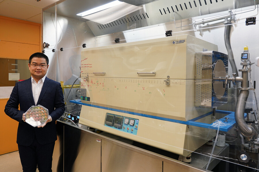
MIT Researchers Grow Transistors on Top of Silicon Wafers

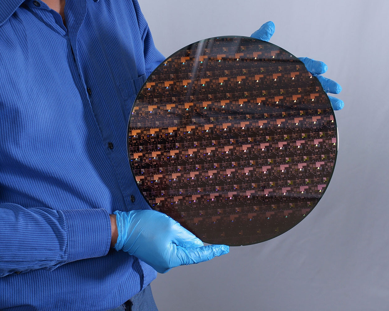
MIT researchers have developed a groundbreaking technology that allows for the growth of 2D transition metal dichalcogenide (TMD) materials directly on fully fabricated silicon chips, enabling denser integrations. Conventional methods require temperatures of about 600°C, which can damage silicon transistors and circuits as they break down above 400°C. The MIT team overcame this challenge by creating a low-temperature growth process that preserves the chip's integrity, allowing 2D semiconductor transistors to be directly integrated on top of standard silicon circuits. The new approach grows a smooth, highly uniform layer across an entire 8-inch wafer, unlike previous methods that involved growing 2D materials elsewhere before transferring them to a chip or wafer. This process often led to imperfections that negatively impacted device and chip performance.

Additionally, the novel technology can grow a uniform layer of TMD material in less than an hour over 8-inch wafers, a significant improvement from previous methods that required over a day for a single layer. The enhanced speed and uniformity of this technology make it suitable for commercial applications, where 8-inch or larger wafers are essential. The researchers focused on molybdenum disulfide, a flexible, transparent 2D material with powerful electronic and photonic properties ideal for semiconductor transistors. They designed a new furnace for the metal-organic chemical vapor deposition process, which has separate low and high-temperature regions. The silicon wafer is placed in the low-temperature region while vaporized molybdenum and sulfur precursors flow into the furnace. Molybdenum remains in the low-temperature region, while the sulfur precursor decomposes in the high-temperature region before flowing back into the low-temperature region to grow molybdenum disulfide on the wafer surface.

TSMC Certifies Ansys Multiphysics Solutions for TSMC's N2 Silicon Process

Ansys and TSMC continue their long-standing technology collaboration to announce the certification of Ansys' power integrity software for TSMC's N2 process technology. The TSMC N2 process, which adopts nanosheet transistor structure, represents a major advancement in semiconductor technology with significant speed and power advantages for high performance computing (HPC), mobile chips, and 3D-IC chiplets. Both Ansys RedHawk-SC and Ansys Totem are certified for power integrity signoff on N2, including the effects of self-heat on long-term reliability of wires and transistors. This latest collaboration builds on the recent certification of the Ansys platform for TSMC's N4 and N3E FinFLEX processes.

"TSMC works closely with our Open Innovation Platform (OIP) ecosystem partners to help our mutual customers achieve the best design results with the full stack of design solutions on TSMC's most advanced N2 process," said Dan Kochpatcharin, head of the Design Infrastructure Management Division at TSMC. "Our latest collaboration with Ansys RedHawk-SC and Totem analysis tools allows our customers to benefit from the significant power and performance improvements of our N2 technology while ensuring predictively accurate power and thermal signoff for the long-term reliability of their designs."

Marvell and AWS Collaborate to Enable Cloud-First Silicon Design

Marvell Technology, Inc., a leader in data infrastructure semiconductor solutions, announced today that it has selected Amazon Web Services, Inc. (AWS) as its cloud provider for electronic design automation (EDA). A cloud-first approach helps Marvell to rapidly and securely scale its service on the world's leading cloud, rise to the challenges brought by increasingly complex chip design processes, and deliver continuous innovation for the expanding needs across the automotive, carrier, data center, and enterprise infrastructure markets it serves. The work extends the longstanding relationship between the two companies—Marvell is also a key semiconductor supplier for AWS, helping the company support the design and rapid delivery of cloud services that best meet customers' demanding requirements.

EDA refers to the specialized and compute-intensive processes used in chip making and is a critical piece of Marvell's R&D. Over the years, the number of transistors on an integrated chip has increased exponentially. Each advance in chip design calls for a calculated application of software modules overseeing logic design, debugging, component placement, wire routing, optimization of time and power consumption, and verification. Due to the computationally intensive nature of EDA workloads, it is no longer cost-effective or timely to run EDA on premises. By powering its EDA with AWS, Marvell leverages an unmatched portfolio of services including secure, elastic, high-performance compute capacity in the cloud to solve challenges around speed, latency, security of IP, and data transfer.

Silicon Wafer Pricing Falling for the First Time in Three Years

Semiconductors are largely made using silicon, even though there are other types of substrates that can be used as well, such as gallium nitride or silicon carbide. However, most semiconductors today are made using silicon wafers, which in turn means that silicon wafers are a key material in the semiconductor industry. Over the past three years, the cost of silicon wafers have increased in pricing, due to higher demand, as there has been a higher demand for semiconductors. However, as there are a limited number of suppliers of silicon wafers, especially at the larger 12-inch size, the increased cost in materials has had an impact on the cost of the final semiconductors.

Reports out of Taiwan are suggesting that the price of 12-, 8- and 6-inch wafers are all starting to see a decline in price. We're talking single digit percentages here and it should be noted that these are spot prices, not contract prices, which are negotiated between the parties a long time before delivery. That said, the fact that the spot prices are point downwards also means that companies with not so great contract pricing are starting to want to renegotiate their contract pricing, as even a small saving here can lead to a bigger saving further down the line. Many IC manufacturers have also asked to pause their contract orders, as the utilisation rate of many foundry nodes are going down, which means the foundries aren't in need of as many wafers as they have ordered. Hopefully this will all lead to lower prices across the board when it comes to semiconductors this year, but it's too early to draw any real conclusions. It's also possible that the end customers won't see any direct benefits from lower costs to the manufacturers.

Alleged Apple M2 Max Performance Figures Show Almost 20% Single-Core Improvement

Apple's ongoing pursuit of leading performance in custom silicon packages continues with each new generation of Apple Silicon. Today, we have alleged Geekbench performance figures of the upcoming M2 Max chip, designed for the upcoming Mac devices. Featuring the same configuration with two E-cores and eight P-cores, the chip is rumored to utilize TSMC's 3 nm design. However, that is yet to be confirmed by Apple, so we don't have the exact information. In the GB5 single-thread test, the CPU set a single-core performance target of 1899 points, while the multi-core score was 8737. While last year's M1 Max chips can reach 1787 single-core and 12826 multi-core scores, these configurations are benchmarked in a Mac Studio, which has better cooling and allows for higher clocks to be achieved.

Apples to apples (pun intended) comparison with the M1 Max chip inside of a MacBook Pro version with presumably the same cooling capacity, which gets 1497 single-core and 11506 multi-core score, the new M2 Max chip is 19.4% faster in single-core results. Multi-core improvements should follow, and this M2 Max result should be different from the final product. We await more benchmarks to confirm this performance increase and the correct semiconductor manufacturing node.

Intel Finally Reveals its Software Defined Silicon as Intel On Demand

Back in September 2021, reports about Intel working on something called SDSi or software defined silicon, started to appear. Now, over a year later, the company has finally launched its SDSi products under the Intel On Demand branding. Back then, we speculated about what features Intel would put behind a paywall and although we were somewhat off track, Intel has put some specific "instructions" behind the paywall on the supported Xeon processors. Specifically, some CPUs will have Quick Assist, Dynamic Load Balancer and Data Streaming Accelerator available as an On Demand feature. Additionally, Intel is also putting its Software Guard Extensions and In-Memory Analytics Accelerator behind the same pay wall.

It appears that these features will be offered as-a-service offering from some of Intel's service partners, but there's also a "one-time activation of select CPU accelerators and security features" according to the Intel On Demand website. It's unclear which Xeon SKUs will get Intel On Demand, but according to The Register, it'll be the upcoming Sapphire Rapids based Xeon processors which should be the first parts affected. Intel has listed partners like HP, Lenovo and SuperMicro, among others, that are involved with the Intel On Demand program. It will still be possible to buy next gen Xeon CPUs that are fully feature enabled like today, but it's unclear if the Intel On Demand Xeon SKUs will offer some kind of cost benefits to companies that don't need the additional features that are behind the paywall.

Report: Apple to Move a Part of its Embedded Cores to RISC-V, Stepping Away from Arm ISA

According to Dylan Patel of SemiAnalysis sources, Apple is moving its embedded cores from Arm to RISC-V. In Apple's Silicon designs, there are far more cores than the main ones that power the operating system and end-user applications. For example, embedded cores are present, and there are 30+ in M1 SoCs responsible for all kinds of workloads not related to the operating system. These tasks are usually associated with other functions such as WiFi/BlueTooth, ThunderBolt retiming, touchpad control, NAND chips having their own core, etc. They run their own firmware and power everything around the central cores that run the OS, so the whole SoC functions appropriately.

It appears that a lot of these cores are based on Arm M-series or lower-end A-series IP that Apple is currently looking to replace with RISC-V. Given that a large portion of software runs on the main big.LITTLE configuration, other secondary SoC tasks can migrate to a different ISA like RISC-V, with a small firmware adjustment. Given that these cores can be placed with custom IPs, Apple would save licensing fees if custom RISC-V cores were used. Additionally, developing firmware for these cores at an Apple engineering team size shouldn't be a problem. Of course, we have no information about when these custom cores will appear inside Apple Silicon. Even when they are used, no formal announcement is expected given that the main cores remain to be powered by Arm ISA, with everything else invisible to the end-user.

POINTek Shows Off Optical Fiber Array Product Families for Silicon Photonics Integrated Chips

POINTek, Inc., a global leader and provider of high performance athermal AWGs, announced launching of new Application- Specific Optical Fiber Array Products, Silicon Photonics (SiPh) Fiber Arrays, which is capable of supporting the back-end packaging for Silicon Photonics Integrated Circuits (PIC). This new Silicon Photonics Fiber Arrays have the excellent characteristics of a fine fiber-end mirror-surface quality and an accurate fiber protrusion length uniformity to match with the prefabricated V-grooves on a Silicon PIC chip. The required fiber protrusion length is typically 5 mm with ≤ ±2 um length uniformity in an array. Both Single Mode (SM) Fiber Arrays and Polarization Maintaining (PM) Fiber Arrays are available with or without 12-channel MT ferrule termination.

"This new SiPh Fiber Array is designed to passively align the multiple optical fibers into the wafer-fabricated V-grooves on the Silicon PIC chip without the expensive and complicated active alignment equipment, and furthermore, the passive alignment of the Array can be accomplished without monitoring the optical power," according to Dr. Donald Yu, CMO of POINTek, operating from Los Angeles, California. Yu explains that the optical fiber array is a key component to efficiently assemble the PIC devices for coupling the multiple fibers into the multiple I/O waveguides on a PIC chip. In the conventional optical active alignment assembly process, the expensive automatic precision alignment equipment should be utilized while monitoring the optical power in the packaging process, and it often takes the long processing time. "However, for this new SiPh Fiber Array, the fibers can be precisely placed in the Silicon PIC's V-grooves with the minimal operation costs. Therefore, the passive alignment of Silicon PIC could result in the very affordable SiPh device price in the market," Yu adds.

MediaTek Announces Commitment to Open New Semiconductor Design Center at Purdue University in Indiana

Today, leading global fabless chipmaker MediaTek Inc., [joined by Indiana Governor Eric J. Holcomb, Deputy Secretary of Commerce Don Graves, Indiana Secretary of Commerce Bradley B. Chambers, and Purdue College of Engineering's Dr. Mung Chiang] announced their commitment to accept a state transition assistance package from the Indiana Economic Development Commission (IEDC) to support its very first Midwest semiconductor chip design center in West Lafayette, Indiana. MediaTek also shared its intention to create a new research partnership with Purdue to collaborate on engineering talent development and new research on next-generation computing and communications chip design. The news was shared with senior leaders, other international investors and policymakers assembled in National Harbor, Maryland for the 2022 SelectUSA Investment Summit.

This novel partnership in Indiana represents a new U.S. growth model for MediaTek USA; outside the traditional centers of gravity for chip design. "We believe strongly that being in Indiana means we'll have access to some of the best engineering talent in the world," said Dr. Kou-Hung Lawrence Loh, Corporate Senior Vice President of MediaTek Inc. and President of MediaTek USA, Inc. "Not just at Purdue, but West Lafayette is only four hours away from nearly a dozen of the top engineering schools in the country. In the post pandemic world, top candidates tell us they want to be closer to home, near family and they want to have a real house and great schools. Indiana offers all that and more."

Apple Reportedly Captures 90% of Arm PC Revenue Share

With the launch of Apple Silicon for Mac computers, Apple has established itself as a great user of the Arm instruction set. Starting with M1, the company released an entirely new family of products running Apple Silicon. Today, thanks to the research of Strategy Analytics company, we have information that Apple is capturing as much as 90% of the revenue share present in the Arm PC market. The Arm PC market is a tiny subset of the entire PC market, mainly equipped with one-off Windows-on-Arm devices, Chromebook PCs, and Apple Macs. With the naturally low prices of the remaining Arm PCs, Apple Arm PCs offer a relatively high price point and a much more incredible selection of products.

On the global scale, Arm PCs now account for 9% of the total PC market share, where x86 vendors are dominating the field. "Apple's M-series family of processors set the benchmark and gave Apple a 2-3-year lead over the rest of the Arm-based PC processor vendors. Qualcomm captured just 3% revenue share in the Arm-based notebook PC processor market in 2021 and lags Apple in CPU performance," said Sravan Kundojjala, Director of Handset Component Technologies service at Strategy Analytics. This points to a particular case of Apple's better product and feeding the demand with higher-performing processors. Qualcomm's acquisition of Nuvia should yield different results in the coming years, as the new IP is yet to appear in Qualcomm SoCs.

Supply Cut of Noble Gases from Russia Could Hit Chip Production

It turns out that Russia was a major supplier of, among many other things, industrial-grade noble gases, which are vital for semiconductor production. Earlier this month, the Russian government announced that it is cutting supply of noble gases to "unfriendly countries" (countries in the US sphere of influence), unless they pay for the merchandise in Russian Rubles, by creating remittance accounts in Russian banks (similar to how it wants these countries to pay for crude oil and natural gas).

Russia and Ukraine were leading global suppliers of industrial noble gases, together making up a third of the noble gas consumed by the semiconductor industry. Much of the heavy industry in Ukraine is either out of service, or committed to the war effort, which lets Russia dictate terms for its supply. Argon, xenon, helium, and neon are the most sought after noble gases in the semiconductor industry. In addition to the inert environment, mixtures of these gases are required by the lasers that perform lithography (etching microscopic circuits on silicon wafer).

Apple M1 Chips Affected by Unpatchable "PACMAN" Exploit

Apple M1 chips are a part of the Apple Silicon family that represents a new transition to Arm-based cores with new power and performance targets for Apple devices. A portion of building a processor is designing its security enclave, and today we have evidence that M1 processors got a new vulnerability. The PACMAN is a hardware attack that can bypass Pointer Authentication (PAC) on M1 processors. Security researchers took an existing concept of Spectre and its application in the x86 realm and now applied it to the Arm-based Apple silicon. PACMAN exploits a current software bug to perform pointer authentication bypass, which may lead to arbitrary code execution.

The vulnerability is a hardware/software co-design that exploits microarchitectural construction to execute arbitrary codes. PACMAN creates a PAC Oracle to check if a specific pointer matches its authentication. It must never crash if an incorrect guess is supplied and the attack brute-forces all the possible PAC values using the PAC Oracle. To suppress crashes, PAC Oracles are delivered speculatively. And to learn if the PAC value was correct, researchers used uArch side channeling. In the CPU resides translation lookaside buffers (TLBs), where PACMAN tries to load the pointer speculatively and verify success using the prime+probe technique. TLBs are filled with minimal addresses required to supply a particular TLB section. If any address is evicted from the TLB, it is likely a load success, and the bug can take over with a falsely authenticated memory address.
Apple M1 PACMAN Attack

AMD Selects Google Cloud to Provide Additional Scale for Chip Design Workloads

Google Cloud and AMD today announced a technology partnership in which AMD will run electronic design automation (EDA) for its chip-design workloads on Google Cloud, further extending the on-premises capabilities of AMD data centers. AMD will also leverage Google Cloud's global networking, storage, artificial intelligence, and machine learning capabilities to further improve upon its hybrid and multicloud strategy for these EDA workloads.

Scale, elasticity, and efficient utilization of resources play critical roles in chip design, particularly given that the demand for compute processing grows with each node advancement. To remain flexible and scale easily, AMD will add Google Cloud's newest compute-optimized C2D VM instance, powered by 3rd Gen AMD EPYC processors, to its suite of resources focused on EDA workloads. By leveraging Google Cloud, AMD anticipates being able to run more designs in parallel, giving the team more flexibility to manage short-term compute demands, without reducing allocation on long-term projects.

Apple Unveils M1 Ultra, the World's Most Powerful Chip For a Personal Computer

Apple today announced M1 Ultra, the next giant leap for Apple silicon and the Mac. Featuring UltraFusion — Apple's innovative packaging architecture that interconnects the die of two M1 Max chips to create a system on a chip (SoC) with unprecedented levels of performance and capabilities — M1 Ultra delivers breathtaking computing power to the new Mac Studio while maintaining industry-leading performance per watt.

The new SoC consists of 114 billion transistors, the most ever in a personal computer chip. M1 Ultra can be configured with up to 128 GB of high-bandwidth, low-latency unified memory that can be accessed by the 20-core CPU, 64-core GPU and 32-core Neural Engine, providing astonishing performance for developers compiling code, artists working in huge 3D environments that were previously impossible to render, and video professionals who can transcode video to ProRes up to 5.6x faster than with a 28-core Mac Pro with Afterburner.

Gartner: Worldwide Semiconductor Revenue Grew 25.1% in 2021, Exceeding $500 Billion For the First Time

Worldwide semiconductor revenue increased 25.1% in 2021 to total $583.5 billion, crossing the $500 billion threshold for the first time, according to preliminary results by Gartner, Inc.

"As the global economy bounced back in 2021, shortages appeared throughout the semiconductor supply chain, particularly in the automotive industry," said Andrew Norwood, research vice president at Gartner. "The resulting combination of strong demand as well as logistics and raw material price increases drove semiconductors' average selling price higher (ASP), contributing to overall revenue growth in 2021.

IBM and Samsung Unveil Semiconductor Breakthrough That Defies Conventional Design

Today, IBM and Samsung Electronics jointly announced a breakthrough in semiconductor design utilizing a new vertical transistor architecture that demonstrates a path to scaling beyond nanosheet, and has the potential to reduce energy usage by 85 percent compared to a scaled fin field-effect transistor (finFET)1. The global semiconductor shortage has highlighted the critical role of investment in chip research and development and the importance of chips in everything from computing, to appliances, to communication devices, transportation systems, and critical infrastructure.

The two companies' semiconductor innovation was produced at the Albany Nanotech Complex in Albany, NY, where research scientists work in close collaboration with public and private sector partners to push the boundaries of logic scaling and semiconductor capabilities. This collaborative approach to innovation makes the Albany Nanotech Complex a world-leading ecosystem for semiconductor research and creates a strong innovation pipeline, helping to address manufacturing demands and accelerate the growth of the global chip industry.

Intel CEO Cites Brexit as Reason for Chip Fab Plans in UK Not an Option

In an interview with the BBC, Intel CEO Pat Gelsinger said that the company is no longer considering the UK as a site for a chip fab, due to Brexit, something the company had apparently done prior to Brexit. Now the company is looking for a location in another EU country for a US$95 billion investment for a new semiconductor plant, as well as upgrades to its current plants in Ireland.

Although Intel had not made any firm decisions on a site location prior to Brexit, Gelsinger is quoted as saying "I have no idea whether we would have had a superior site from the UK, but we now have about 70 proposals for sites across Europe from maybe 10 different countries." He continues "We're hopeful that we'll get to agreement on a site, as well as support from the EU... before the end of this year."

HiSilicon Develops RISC-V Processor to Move Away from Arm Restrictions

Huawei's HiSilicon subsidiary, which specialized in the design and development of semiconductor devices like processors, has made a big announcement today. A while back, the US government has blacklisted Huawei from using any US-made technology. This has rendered HiSilicon's efforts of building processors based on Arm architecture (ISA) practically useless, as the US sanctions applied to that as well. So, the company had to turn to alternative technologies. Today, HiSilicon has announced the new HiSilicon Hi3861 development board, based on RISC-V architecture. This represents an important step to Huawei's silicon independence, as RISC-V is a free and open-source ISA designed for all kinds of workloads.

While the HiSilicon Hi3861 development board features a low-power Hi3861 chip, it is the company's first attempt at building a RISC-V design. It features a "high-performance 32-bit microprocessor with a maximum operating frequency of 160 MHz". While this may sound very pale in comparison to the traditional HiSilicon products, this chip is used for IoT applications, which don't require much processing power. For tasks that need better processing, HiSilicon will surely develop more powerful designs. This just represents an important starting point, where Huawei's HiSilicon moves away from Arm ISA, and steps into another ISA design and development. This time, with RISC-V, the US government has no control over the ISA, as it is free to use by anyone who pleases, with added benefits of no licensing costs. It is interesting to see where this will lead HiSilicon and what products the company plans to release on the new ISA.

Raytheon Technologies and GLOBALFOUNDRIES Partner to Accelerate 5G Wireless Connectivity Using Gallium Nitride on Silicon (GaN-on-Si)

Raytheon Technologies (NYSE: RTX), a leading aerospace and defense technology company, and GLOBALFOUNDRIES (GF ), the global leader in feature-rich semiconductor manufacturing, will collaborate to develop and commercialize a new gallium nitride on silicon (GaN-on-Si) semiconductor that will enable game-changing radio frequency performance for 5G and 6G mobile and wireless infrastructure applications.

Under the agreement, Raytheon Technologies will license its proprietary gallium nitride on silicon technology and technical expertise to GF, which will develop the new semiconductor at its Fab 9 facility in Burlington, Vermont. Gallium nitride is a unique material used to build high-performance semiconductors that can handle significant heat and power levels. This makes it ideal to handle 5G and 6G wireless signals, which require higher performance levels than legacy wireless systems.

IBM Announces World's First 2nm Chip Technology

IBM today unveiled a breakthrough in semiconductor design and process with the development of the world's first chip announced with 2 nanometer (nm) nanosheet technology. Semiconductors play critical roles in everything from computing, to appliances, to communication devices, transportation systems, and critical infrastructure.

Demand for increased chip performance and energy efficiency continues to rise, especially in the era of hybrid cloud, AI, and the Internet of Things. IBM's new 2 nm chip technology helps advance the state-of-the-art in the semiconductor industry, addressing this growing demand. It is projected to achieve 45 percent higher performance, or 75 percent lower energy use, than today's most advanced 7 nm node chips.

Tenstorrent Selects SiFive Intelligence X280 for Next-Generation AI Processors

SiFive, Inc., the industry leader in RISC-V processors and silicon solutions, today announced that Tenstorrent, an AI semiconductor and software start-up developing next-generation computers, will license the new SiFive Intelligence X280 processor in its AI training and inference processor. SiFive will deliver more details of its SiFive Intelligence initiative including the SiFive Intelligence X280 processor at the Linley Spring Processor Conference on April 23rd.

Tenstorrent's novel approach to inference and training effectively and efficiently accommodates the exponential growth in the size of machine learning models while offering best-in-class performance.

TSMC to Enter 4 nm Node Volume Production in Q4 of 2021

TSMC, the world leader in semiconductor manufacturing, has reportedly begun with plans to start volume production of the 4 nm node by the end of this year. According to the sources over at DigiTimes, Taiwan's leading semiconductor manufacturer could be on the verge of starting volume production of an even smaller node. The new 4 nm node is internally referred to as a part of the N5 node generation. The N5 generation covers N5 (regular 5 nm), N5P (5 nm+), and N4 process that is expected to debut soon. And perhaps the most interesting thing is that the 4 nm process will be in high-volume production in Q4, with Apple expected to be one of the major consumers of the N5 node family.

DigiTimes reports that Apple will use the N5P node for the upcoming Apple A15 SoCs for next-generation iPhones, while the more advanced N4 node will find itself as a base of the new Macs equipped with custom Apple Silicon SoCs. To find out more, we have to wait for the official product launches and see just how much improvement new nodes bring.

Apple Mac Pro 2022 Rumored to Feature Custom 64-Core Processor & Sell For 19,000 USD

Apple relaunched the Mac Pro in 2019 with a return to the original tower form factor and packing 24-core Intel Xeon-W processors paired with AMD Radeon Pro Vega GPUs. Apple is reportedly planning to release a fourth-generation Mac Pro in 2022 with the most powerful Apple silicon yet. The 2022 Mac Pro will be available in three base configurations with 32, 48, and 64 core versions featuring new processors developed by Apple with similar performance and power-efficient core designs as found in the Apple M1.

The entry-level 32 core model will include 24 high-performance cores, 32 GPU cores, 64 GB ram, and will start at 5,499 USD. The mid-range 48 core model will include 36 high-performance cores, 64 GPU cores, 256 GB ram, and will start at 11,999 USD. The highest-end 64 core model will include 48 high-performance cores, 128 GPU cores, 512 GB ram, and will start at 18,999 USD. Storage options will vary from 512 GB to 8 TB of SSD storage as is currently available. These machines are shaping up to be some of the most powerful prosumer computers available if these rumors are true.

Apple is Discontinuing Intel-based iMac Pro

According to the official company website, Apple will no longer manufacture its iMac Pro computers based on Intel processors. Instead, the company will carry these models in its store, only while the supplies last. Apple will be replacing these models with next-generation iMac Pro devices that will be home to the custom Apple Silicon processors, combining Arm CPU cores with custom GPU design. Having a starting price of 4990 USD, the Apple iMac Pro was able to max out at 15000 USD. The most expensive part was exactly the Intel Xeon processor inside it, among the AMD GPU with HBM. Configuration pricing was also driven by storage/RAM options. However, even the most expensive iMac Pro with its 2017 hardware had no chance against the regular 2020 iMac, so the product was set to be discontinued sooner or later.

When the stock of the iMac Pro runs out, Apple will replace this model with its Apple Silicon equipped variant. According to the current rumor mill, Apple is set to hold a keynote on March 16th that will be an announcement for new iMac Pro devices with custom processors. What happens is only up to Apple, so we have to wait and see.

ADATA Explains Changes with XPG SX8200 Pro SSD

ADATA has recently been in a spot of controversy when it comes to their XPG SX8200 Pro solid-state drive (SSD). The company has reportedly shipped many different configurations of the SSD with different drive controller clock speeds and different NAND flash. According to the original report, ADATA has first shipped the SX8200 Pro SSD with Silicon Motion SM2262ENG SSD controller, running at 650 MHz with IMFT 64-layer TLC NAND Flash. However, it was later reported that the SSD was updated to use the Silicon Motion SM2262G SSD controller, clocked at 575 MHz. With this report, many users have gotten concerned and started to question the company's practices. However, ADATA later ensured everyone that performance is within the specifications and there is no need to worry.

Today, we have another report about the ADATA XPG SX8200 Pro SSD. According to a Redditor, ADATA has once again updated its SSD with a different kind of NAND Flash, however, this time the report indicated that performance was impacted. Tom's Hardware has made a table of changes showing as many as five revisions of the SSD, all with different configurations of SSD controllers and NAND Flash memory. We have contacted ADATA to clarify the issues that have emerged, and this is the official response that the company gave us.
Return to Keyword Browsing
May 15th, 2024 22:41 EDT change timezone

New Forum Posts

Popular Reviews

Controversial News Posts