Linux Gets Ported to Apple's M1-Based Devices
When Apple introduces its lineup of devices based on the custom Apple Silicon, many people have thought that it represents the end for any further device customization and that Apple is effectively locking-up the ecosystem even more. That is not the case we have today. Usually, developers working on Macs are always in need of another operating system to test their software and try it out. It means that they have to run some virtualization software like virtual machines to test another OS like Linux and possibly Windows. However, it would be a lot easier if they could just boot that OS directly on the device and that is exactly why we are here today.
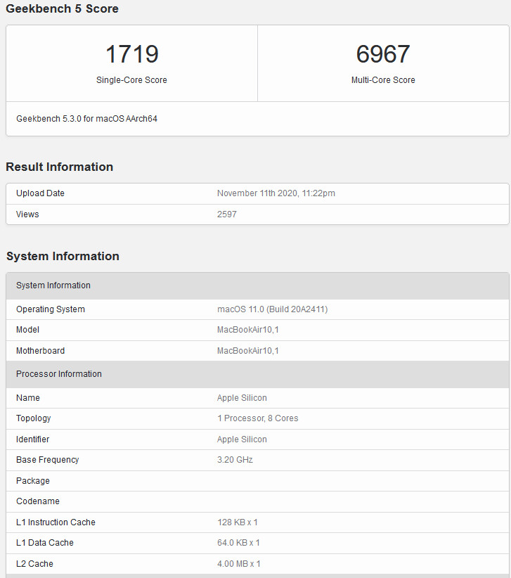
Researchers from Corellium, a startup company based in Florida, working on ARM device virtualization, have pulled off an incredible feat. They have managed to get Linux running on Apple's M1 custom silicon based devices. The CTO of Corellium, Mr. Chris Wade, has announced that Linux is now fully usable on M1 silicon. The port can take full advantage of the CPU, however, there is no GPU acceleration for now, and graphics are set to the software rendering mode. Corellium also promises to take the changes it made upstream to the Linux kernel itself, meaning open-source and permissive license model. Below you can find an image of Apple M1 Mac Mini running the latest Ubuntu OS build.

Researchers from Corellium, a startup company based in Florida, working on ARM device virtualization, have pulled off an incredible feat. They have managed to get Linux running on Apple's M1 custom silicon based devices. The CTO of Corellium, Mr. Chris Wade, has announced that Linux is now fully usable on M1 silicon. The port can take full advantage of the CPU, however, there is no GPU acceleration for now, and graphics are set to the software rendering mode. Corellium also promises to take the changes it made upstream to the Linux kernel itself, meaning open-source and permissive license model. Below you can find an image of Apple M1 Mac Mini running the latest Ubuntu OS build.