News Posts matching #SoC

Return to Keyword Browsing

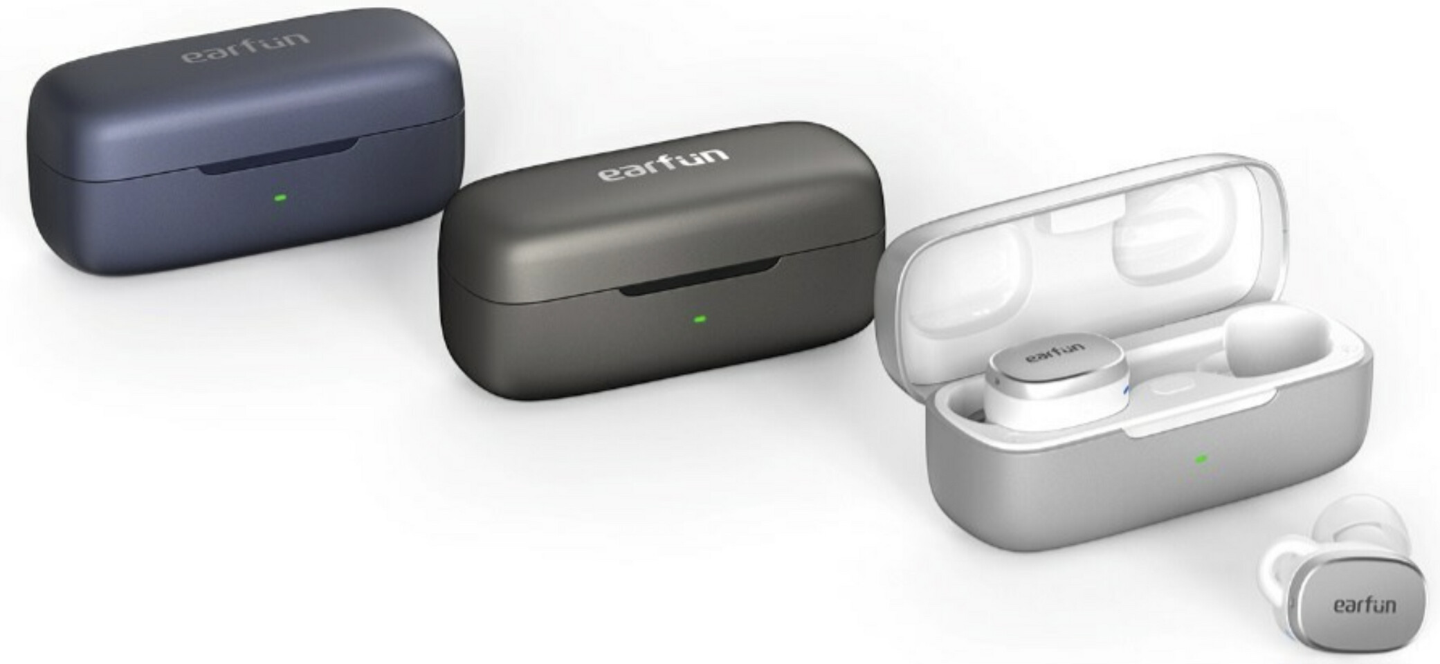
EarFun Announces the Free Pro 3 - The World's First Snapdragon Sound and Hi-Res ANC Earbuds

EarFun's development kitchen remains hot. Delivering their first IEM and portable USB-C DAC just this past month, the awarded audio brand will be releasing the next generational leap from their current lineup, the Free Pro 3.

Revolutionizing True Wireless Audio and Noise Cancelation
The new true wireless earbuds are the first pair of earbuds that combine Snapdragon Sound Certification, Hi-Res audio, Qualcomm's QCC3072 SoC, the latest v5.3 Bluetooth certification, Low-Energy Audio protocol, and aptX Adaptive technology. It will also feature EarFun's proprietary QuietSmart 2.0 technology for active noise cancellation up to 43dB, and 6-mic cVc call noise-reduction. It will boast a generous battery life of up to 33 hours, an IPX5 certification, wireless charging, and multipoint connectivity. The Free Pro 3 will make use of EarFun's customizable audio app for total user configuration.

Renesas Unveils the First Generation of Own 32-bit RISC-V CPU Core Ahead of Competition

Renesas Electronics Corporation, a premier supplier of advanced semiconductor solutions, announced today that it has designed and tested a 32-bit CPU core based on the open-standard RISC-V instruction set architecture (ISA). Renesas is among the first in the industry to independently develop a CPU core for the 32-bit general-purpose RISC-V market, providing an open and flexible platform for IoT, consumer electronics, healthcare and industrial systems. The new RISC-V CPU core will complement Renesas' existing IP portfolio of 32-bit microcontrollers (MCUs), including the proprietary RX Family and the RA Family based on the Arm Cortex -M architecture.

RISC-V is an open ISA which is quickly gaining popularity in the semiconductor industry, due to its flexibility, scalability, power efficiency and open ecosystem. While many MCU providers have recently created joint investment alliances to accelerate their development of RISC-V products, Renesas has already developed a new RISC-V core on its own. This versatile CPU can serve as a main application controller, a complementary secondary core in SoCs, on-chip subsystems, or even in deeply embedded ASSPs. This positions Renesas as a leader in the emerging RISC-V market, following previous introductions of its 32-bit voice-control and motor-control ASSP devices, as well as the RZ/Five 64-bit general purpose microprocessors (MPUs), which were built on CPU cores developed by Andes Technology Corp.

Manufacturers Anticipate Completion of NVIDIA's HBM3e Verification by 1Q24; HBM4 Expected to Launch in 2026

TrendForce's latest research into the HBM market indicates that NVIDIA plans to diversify its HBM suppliers for more robust and efficient supply chain management. Samsung's HBM3 (24 GB) is anticipated to complete verification with NVIDIA by December this year. The progress of HBM3e, as outlined in the timeline below, shows that Micron provided its 8hi (24 GB) samples to NVIDIA by the end of July, SK hynix in mid-August, and Samsung in early October.

Given the intricacy of the HBM verification process—estimated to take two quarters—TrendForce expects that some manufacturers might learn preliminary HBM3e results by the end of 2023. However, it's generally anticipated that major manufacturers will have definite results by 1Q24. Notably, the outcomes will influence NVIDIA's procurement decisions for 2024, as final evaluations are still underway.

Microsoft Introduces 128-Core Arm CPU for Cloud and Custom AI Accelerator

During its Ignite conference, Microsoft introduced a duo of custom-designed silicon made to accelerate AI and excel in cloud workloads. First of the two is Microsoft's Azure Cobalt 100 CPU, a 128-core design that features a 64-bit Armv9 instruction set, implemented in a cloud-native design that is set to become a part of Microsoft's offerings. While there aren't many details regarding the configuration, the company claims that the performance target is up to 40% when compared to the current generation of Arm servers running on Azure cloud. The SoC has used Arm's Neoverse CSS platform customized for Microsoft, with presumably Arm Neoverse N2 cores.

The next and hottest topic in the server space is AI acceleration, which is needed for running today's large language models. Microsoft hosts OpenAI's ChatGPT, Microsoft's Copilot, and many other AI services. To help make them run as fast as possible, Microsoft's project Athena now has the name of Maia 100 AI accelerator, which is manufactured on TSMC's 5 nm process. It features 105 billion transistors and supports various MX data formats, even those smaller than 8-bit bit, for maximum performance. Currently tested on GPT 3.5 Turbo, we have yet to see performance figures and comparisons with competing hardware from NVIDIA, like H100/H200 and AMD, with MI300X. The Maia 100 has an aggregate bandwidth of 4.8 Terabits per accelerator, which uses a custom Ethernet-based networking protocol for scaling. These chips are expected to appear in Microsoft data centers early next year, and we hope to get some performance numbers soon.

Synopsys Expands Its ARC Processor IP Portfolio with New RISC-V Family

Synopsys, Inc. (Nasdaq: SNPS) today announced it has extended its ARC Processor IP portfolio to include new RISC-V ARC-V Processor IP, enabling customers to choose from a broad range of flexible, extensible processor options that deliver optimal power-performance efficiency for their target applications. Synopsys leveraged decades of processor IP and software development toolkit experience to develop the new ARC-V Processor IP that is built on the proven microarchitecture of Synopsys' existing ARC Processors, with the added benefit of the expanding RISC-V software ecosystem.

Synopsys ARC-V Processor IP includes high-performance, mid-range, and ultra-low power options, as well as functional safety versions, to address a broad range of application workloads. To accelerate software development, the Synopsys ARC-V Processor IP is supported by the robust and proven Synopsys MetaWare Development Toolkit that generates highly efficient code. In addition, the Synopsys.ai full-stack AI-driven EDA suite is co-optimized with ARC-V Processor IP to provide an out-of-the-box development and verification environment that helps boost productivity and quality-of-results for ARC-V-based SoCs.

MediaTek Announces the Dimensity 9300 Flagship SoC, with Big Cores Only

MediaTek today announced the Dimensity 9300, its newest flagship mobile chip with a one-of-a-kind All Big Core design. The unique configuration combines extreme performance with MediaTek's industry-leading power efficiency to deliver unmatched user experiences in gaming, video capture and on-device generative AI processing.

"The Dimensity 9300 is MediaTek's most powerful flagship chip yet, bringing a huge boost in raw computing power to flagship smartphones with our groundbreaking All Big Core design," said Joe Chen, President at MediaTek. "This unique architecture, combined with our upgraded on-chip AI Processing Unit, will usher in a new era of generative AI applications as developers push the limits with edge AI and hybrid AI computing capabilities."

AMD FidelityFX Super Resolution Could Come to Samsung and Qualcomm SoCs

AMD FidelityFX Super Resolution (FSR) is an open-source resolution upscaling technology that takes lower-resolution input and uses super-resolution temporal upscaling technology, frame generation using AMD Fluid Motion Frames (AFMF) technology, and built-in latency reduction technology to provide greater-resolution output images from lower-resolution settings. While the technology is open-source, it battles in market share with NVIDIA and the company's Deep Learning Super Sampling (DLSS). However, in the mobile space, there hasn't been much talk about implementing upscaling technology up until now. According to a popular leaker @Tech_Reve on X/Twitter, we have information that AMD is collaborating with Samsung and Qualcomm to standardize on upscaling technology implementations in mobile SoCs.

Not only does the leak imply that the AMD FSR technology will be used in Samsung's upcoming Exynos SoC, but some AMD ray tracing will be present as well. The leaker has mentioned Qualcomm, which means that future iterations of Snapdragon are up to adopt the FSR algorithmic approach to resolution upscaling. We will see how and when, but with mobile games growing in size and demand, FSR could come in handy to provide mobile gamers with a better experience. Primarily, this targets Android devices, which Qualcomm supplies, where Apple's iPhone recently announced MetalFX Upscaling technology with an A17 Pro chip.

BeagleBoard.org Announces New BeagleV-Fire FPGA and RISC-V Single Board Computer

BeagleBoard.org, a pioneer in open-source single-board computers (SBCs), is excited to unveil the BeagleV -Fire, a revolutionary SBC powered by the Microchip's PolarFire MPFS025T FCVG484E 5x core RISC-V System on Chip (SoC) with FPGA fabric. This remarkable addition to the BeagleBoard.org BeagleV family of boards opens up new horizons for developers, tinkerers, and the open-source community to explore the vast potential of RISC-V architecture and FPGA technology.

BeagleV -Fire is the second board in the BeagleV series of single board computers (SBCs) from BeagleBoard.org. BeagleV -Fire like other BeagleV SBCs, is set to revolutionize the world of embedded systems and empower developers and enthusiasts worldwide. After the launch of BeagleV -Ahead, BeagleV -Fire represents another significant milestone in the democratization of computer architecture and open-source hardware development for the masses. Built around the powerful and energy-efficient RISC-V instruction set architecture (ISA) along with its versatile FPGA fabric, BeagleV -Fire SBC offers unparalleled opportunities for developers, hobbyists, and researchers to explore and experiment with RISC-V technology.

Qualcomm Launches Premium Snapdragon 8 Gen 3 to Bring Generative AI to the Next Wave of Flagship Smartphones

At Snapdragon Summit, Qualcomm Technologies, Inc. today announced its latest premium mobile platform, the Snapdragon 8 Gen 3—a true titan of on-device intelligence, premium-tier performance, and power efficiency. As the premium Android smartphone SoC leader, Qualcomm Technologies' latest processor will be adopted for flagship devices by global OEMs and smartphone brands including ASUS, Honor, iQOO, MEIZU, NIO, Nubia, OnePlus, OPPO, realme, Redmi, RedMagic, Sony, vivo, Xiaomi, and ZTE.

"Snapdragon 8 Gen 3 infuses high-performance AI across the entire system to deliver premium-level performance and extraordinary experiences to consumers. This platform unlocks a new era of generative AI enabling users to generate unique content, help with productivity, and other breakthrough use cases." said Chris Patrick, senior vice president and general manager of mobile handsets, Qualcomm Technologies, Inc. "Each year, we set out to design leading features and technologies that will power our latest Snapdragon 8-series mobile platform and the next generation of flagship Android devices. The Snapdragon 8 Gen 3 delivers."

Qualcomm Snapdragon Elite X SoC for Laptop Leaks: 12 Cores, LPDDR5X Memory, and WiFi7

Thanks to the information from Windows Report, we have received numerous details regarding Qualcomm's upcoming Snapdragon Elite X chip for laptops. The Snapdragon Elite X SoC is built on top of Nuvia-derived Oryon cores, which Qualcomm put 12 off in the SoC. While we don't know their base frequencies, the all-core boost reaches 3.8 GHz. The SoC can reach up to 4.3 GHz on single and dual-core boosting. However, the slide notes that this is all pure "big" core configuration of the SoC, so no big.LITTLE design is done. The GPU part of Snapdragon Elite X is still based on Qualcomm's Adreno IP; however, the performance figures are up significantly to reach 4.6 TeraFLOPS of supposedly FP32 single-precision power. Accompanying the CPU and GPU, there are dedicated AI and image processing accelerators, like Hexagon Neural Processing Unit (NPU), which can process 45 trillion operations per second (TOPS). For the camera, the Spectra Image Sensor Processor (ISP) is there to support up to 4K HDR video capture on a dual 36 MP or a single 64 MP camera setup.

The SoC supports LPDDR5X memory running at 8533 MT/s and a maximum capacity of 64 GB. Apparently, the memory controller is an 8-channel one with a 16-bit width and a maximum bandwidth of 136 GB/s. Snapdragon Elite X has PCIe 4.0 and supports UFS 4.0 for outside connection. All of this is packed on a die manufactured by TSMC on a 4 nm node. In addition to marketing excellent performance compared to x86 solutions, Qualcomm also advertises the SoC as power efficient. The slide notes that it uses 1/3 of the power at the same peak PC performance of x86 offerings. It is also interesting to note that the package will support WiFi7 and Bluetooth 5.4. Officially coming in 2024, the Snapdragon Elite X will have to compete with Intel's Meteor Lake and/or Arrow Lake, in addition to AMD Strix Point.

Samsung Electronics Holds Memory Tech Day 2023 Unveiling New Innovations To Lead the Hyperscale AI Era

Samsung Electronics Co., Ltd., a world leader in advanced memory technology, today held its annual Memory Tech Day, showcasing industry-first innovations and new memory products to accelerate technological advancements across future applications—including the cloud, edge devices and automotive vehicles.

Attended by about 600 customers, partners and industry experts, the event served as a platform for Samsung executives to expand on the company's vision for "Memory Reimagined," covering long-term plans to continue its memory technology leadership, outlook on market trends and sustainability goals. The company also presented new product innovations such as the HBM3E Shinebolt, LPDDR5X CAMM2 and Detachable AutoSSD.

Socionext Announces Collaboration with Arm and TSMC on 2nm Multi-Core Leading CPU Chiplet Development

Socionext today announced a collaboration with Arm and TSMC for the development of an innovative power-optimized 32-core CPU chiplet in TSMCʼs 2 nm silicon technology, delivering scalable performance for hyperscale data center server, 5/6G infrastructure, DPU and edge-of- network markets.

The engineering samples are targeted to be available in 1H2025. This advanced CPU chiplet proof-of-concept using Arm Neoverse CSS technology is designed for single or multiple instantiations within a single package, along with IO and application-specific custom chiplets to optimize performance for a variety of end applications.

Zero ASIC Democratizing Chip Making

Zero ASIC, a semiconductor startup, came out of stealth today to announce early access to its one-of-a-kind ChipMaker platform, demonstrating a number of world firsts:
  • 3D chiplet composability enabling billions of new silicon products
  • Fully automated no-code chiplet-based chip design
  • Zero install interactive RTL-based chip emulation
  • Roadmap to 100X reduction in chip development costs
"Custom Application Specific Integrated Circuits (ASICs) offer 10-100X cost and energy advantage over commercial off the shelf (COTS) devices, but the enormous development cost makes ASICs non-viable for most applications," said Andreas Olofsson, CEO and founder of Zero ASIC. "To build the next wave of world changing silicon devices, we need to reduce the barrier to ASICs by orders of magnitude. Our mission at Zero ASIC is to make ordering an ASIC as easy as ordering catalog parts from an electronics distributor."

Arm and Synopsys Strengthen Partnership to Accelerate Custom Silicon on Advanced Nodes

Synopsys today announced it has expanded its collaboration with Arm to provide optimized IP and EDA solutions for the newest Arm technology, including the Arm Neoverse V2 platform and Arm Neoverse Compute Subsystem (CSS). Synopsys has joined Arm Total Design where Synopsys will leverage their deep design expertise, the Synopsys.ai full-stack AI-driven EDA suite, and Synopsys Interface, Security, and Silicon Lifecycle Management IP to help mutual customers speed development of their Arm-based CSS solutions. The expanded partnership builds on three decades of collaboration to enable mutual customers to quickly develop specialized silicon at lower cost, with less risk and faster time to market.

"With Arm Total Design, our aim is to enable rapid innovation on Arm Neoverse CSS and engage critical ecosystem expertise at every stage of SoC development," said Mohamed Awad, senior vice president and general manager, Infrastructure Line of Business at Arm. "Our deep technical collaboration with Synopsys to deliver pre-integrated and validated IP and EDA tools will help our mutual customers address the industry's most complex computing challenges with specialized compute."

Comcast and Broadcom to Develop the World's First AI-Powered Access Network With Pioneering New Chipset

Comcast and Broadcom today announced joint efforts to develop the world's first AI-powered access network with a new chipset that embeds artificial intelligence (AI) and machine learning (ML) within the nodes, amps and modems that comprise the last few miles of Comcast's network. With these new capabilities broadly deployed throughout the network, Comcast will be able to transform its operations by automating more network functions and deliver an improved customer experience through better and more actionable intelligence.

Additionally, the new chipset will be the first in the world to incorporate DOCSIS 4.0 Full Duplex (FDX), Extended Spectrum (ESD) and the ability to run both simultaneously, enabling Internet service providers across the globe to deliver DOCSIS 4.0 services using a toolkit with technology options to meet their business needs. DOCSIS 4.0 is the next-generation network technology that will introduce symmetrical multi-gigabit Internet speeds, lower latency, and even better security and reliability to hundreds of millions of people and businesses over their existing connections without the need for major construction of new network infrastructure.

MaxLinear Announces Availability of Puma 8, its DOCSIS 4.0 Cable Modem and Gateway Platform

MaxLinear, Inc., a leader in broadband access solutions, today announced the availability of its DOCSIS 4.0 SoC cable modem and gateway platform, Puma 8. Puma 8 builds on the success of its DOCSIS 3.0 and 3.1 predecessors (Puma 6 and 7) and includes all critical elements of a DOCSIS platform, including a low-power, ultra-high split upstream PGA. The platform is compliant to the DOCSIS 4.0 frequency division duplex (FDD) specification and enables immediate large-scale deployments as a DOCSIS 3.1 device with gradual feature expansion options without the need for costly CPE replacements. Complete modem, Embedded Multimedia Terminal Adapter (EMTA), and gateway platforms will be available from MaxLinear's early access OEM partners in 2024.

MaxLinear's DOCSIS 4.0 platform stands out in the market as an energy-efficient, performance-optimized solution. It aligns perfectly with the deployment strategies and technology requirements of leading MSOs. The Puma 8 platform has been specifically tailored to support Extended Spectrum DOCSIS (ESD)/Frequency Division Duplex (FDD), and it boasts a range of energy-saving features. Even at full utilization, its power consumption is impressively low, at just 20-25 W, which is almost half that of competing solutions. This low power consumption enables a fan-less design, resulting in not only cost savings but also space conservation. To achieve peak performance with industry-leading low power consumption, MaxLinear employed a collaborative co-design approach, encompassing the DOCSIS SoC, AnyWAN SoC, and the programmable gain amplifier (PGA).

Intel Core Ultra 9 185H Appears with 16C/22T Configuration at 5.1 GHz

Intel's upcoming Meteor Lake processor family will see the light of the day in mobile version only, with a big re-brand of the Intel Core i naming structure. Slated for a December 14th launch, we are eager to see the official performance figures. However, we are in for a treat today as we have some early performance figures thanks to Geekbench. According to the GB5 run found by BenchLeaks, Intel's Core Ultra 9 185H CPU has appeared to show its configuration, early performance, and boost frequency that is reaching beyond the 5.0 GHz mark.

As the GB5 run suggests, Core Ultra 9 185H is a 16-core CPU with 22 threads, running at 2.5 GHz base frequency. There are six P-cores, eight E-cores, and two SoC-cores on the package of this SKU. During boost, the CPU can reach up to 5.1 GHz and was paired with 64 GB of DDR5 memory. Interestingly, the CPU scored 1849 points in single-threaded tests and 9832 points in multi-threaded tests, which currently doesn't beat top-end Intel mobile HX SKU like i9-13980HX. However, we estimate this was an early engineering sample, and the final product will be more performant.

Qualcomm Oryon PC SoC to be Rebranded as "Snapdragon X"

Qualcomm is poised to significantly rebrand its PC chip lineup as it transitions from the existing 8cx series to the Snapdragon X Series, designed to differentiate its PC chips from Snapdragon processors in mobile devices. The new Snapdragon X Series will incorporate Qualcomm's Oryon CPU SKU, based on Nuvia's IP and praised for its advanced performance and power efficiency. In addition to the new CPU core, Qualcomm also plans to use a dedicated NPU for accelerating on-device AI applications. However, questions remain regarding the reactions of hardware partners, particularly in response to Qualcomm's request for proprietary power management integrated circuits (PMICs) to be used alongside Oryon SoCs.

This strategic rebranding also entails new logos and badges for the system, symbolizing the shift in the product lineup, and the company plans to introduce a simplified tiering structure for its PC ecosystem. Qualcomm currently holds a dominant position as an Arm-based SoC manufacturer for Windows-on-Arm devices. With this rebranding, Qualcomm hopes to position itself competitively in performance and in marketing as well, with established PC chip providers like AMD and Intel, potentially expanding Arm's market share in the PC industry. Further insights and details regarding the Snapdragon X Series will be revealed during the forthcoming Snapdragon Summit, scheduled from October 24 to 26.

Winbond Introduces Innovative CUBE Architecture for Powerful Edge AI Devices

Winbond Electronics Corporation, a leading global supplier of semiconductor memory solutions, has unveiled a powerful enabling technology for affordable Edge AI computing in mainstream use cases. The Company's new customized ultra-bandwidth elements (CUBE) enable memory technology to be optimized for seamless performance running generative AI on hybrid edge/cloud applications.

CUBE enhances the performance of front-end 3D structures such as chip on wafer (CoW) and wafer on wafer (WoW), as well as back-end 2.5D/3D chip on Si-interposer on substrate and fan-out solutions. Designed to meet the growing demands of edge AI computing devices, it is compatible with memory density from 256 Mb to 8 Gb with a single die, and it can also be 3D stacked to enhance bandwidth while reducing data transfer power consumption.

Report: Qualcomm Forces OEMs to Use Its Own PMICs for Oryon SoC

According to SemiAccurate, Qualcomm is currently navigating through many challenges with its Oryon SoC for laptops. The current problem is that Qualcomm is insisting on integrating its own PMICs (Power Management Integrated Circuits), which are inherently designed for cell phones, causing significant compatibility and efficiency issues. This approach is reported to have led to escalated costs and disagreements with OEMs (Original Equipment Manufacturers), seemingly hindering Qualcomm's foothold in the laptop sector. These PMICs are highlighted as unsuitable and highly priced, requiring the adoption of high-density interconnect (HDI) PCBs engineered explicitly for cell phones, thus not designed to meet the current requirements of laptops optimally. The subsequent spike in production costs has ignited conflicts with OEMs, with several contemplating withdrawing from the project.

In response to the rising tensions, Qualcomm is allegedly providing financial compensation to the OEMs, potentially leading to selling SoCs at cost. The only good thing is the reported success of Nuvia-based Oryon SoC. The silicon is perfect at A0 stepping, and performance is reportedly good. However, power usage and efficiency are still in question. Forcing OEMs to use proprietary PMICs will likely have far-reaching impacts on Qualcomm's market strategies and relationships with OEMs. With disputes like this, we expect that Qualcomm-powered laptops are nearing availability, and we could see them in the coming months.

Q2 Revenue for Top 10 Global IC Houses Surges by 12.5% as Q3 on Pace to Set New Record

Fueled by an AI-driven inventory stocking frenzy across the supply chain, TrendForce reveals that Q2 revenue for the top 10 global IC design powerhouses soared to US $38.1 billion, marking a 12.5% quarterly increase. In this rising tide, NVIDIA seized the crown, officially dethroning Qualcomm as the world's premier IC design house, while the remainder of the leaderboard remained stable.

AI charges ahead, buoying IC design performance amid a seasonal stocking slump
NVIDIA is reaping the rewards of a global transformation. Bolstered by the global demand from CSPs, internet behemoths, and enterprises diving into generative AI and large language models, NVIDIA's data center revenue skyrocketed by a whopping 105%. A deluge of shipments, including the likes of their advanced Hopper and Ampere architecture HGX systems and the high-performing InfinBand, played a pivotal role. Beyond that, both gaming and professional visualization sectors thrived under the allure of fresh product launches. Clocking a Q2 revenue of US$11.33 billion (a 68.3% surge), NVIDIA has vaulted over both Qualcomm and Broadcom to seize the IC design throne.

Intel 288 E-core Xeon "Sierra Forest" Out to Eat AMD EPYC Bergamo's Lunch

Intel at the 2023 InnovatiON event unveiled a 288-core extreme core-count variant of the Xeon "Sierra Forest" processor for high-density servers for scale-out, cloud-native environments. It succeeds the current 144-core model. "Sierra Forest" is a server processor based entirely on efficiency cores, or E-cores, based on the "Sierra Glen" core microarchitecture, a server-grade derivative of "Crestmont," Intel's second-generation E-core that's making a client debut with "Meteor Lake."

Xeon "Sierra Forest" is a chiplet-based processor, much like "Meteor Lake" and the upcoming "Emerald Rapids" server processor. It features a total of five tiles—two Compute tiles, two I/O tiles, and a base tile (interposer). Each of the two Compute tiles is built on the Intel 3 foundry node, a more advanced node than Intel 4, featuring higher-density libraries, and an undisclosed performance/Watt increase. Each tile has 36 "Sierra Glen" E-core clusters, 108 MB of shared L3 cache, 6-channel (12 sub-channel) DDR5 memory controllers, and Foveros tile-to-tile interfaces.

Arm IPO Filing Reveals Development of Reference Designs

British semiconductor specialist firm, Arm Ltd., has has confirmed that it will be offering its clients the option to license "SoC solutions," as opposed to the usual model of paying for intellectual properties. A new Bloomberg article reaffirms previous claims that Arm's engineering department was beavering away on reference chip designs. An IPO filing, registered with the SEC, reveals that various system-on-chip designs are in the pipeline—likely targeting fast-growing tech markets.

An Arm statement explained: "More recently, we have invested in a holistic, solution-focused approach to design, expanding beyond individual design IP elements to providing a more complete system. By delivering SoC solutions optimized for specific use cases, we can ensure that the entire system works together seamlessly to provide maximum performance and efficiency. At the same time, by designing an increasingly greater portion of the overall chip design, we are further reducing incremental development investment and risk borne by our customers while also enabling us to capture more value per device." Arm is probably keen to boost its profit margins, and become more attractive in the eyes of potential investors—lately their designs have been implemented in more expensive product segments, namely automotive, client PCs, and cloud data center solutions.

MediaTek Successfully Develops First Chip Using TSMC's 3 nm Process, Set for Volume Production in 2024

MediaTek and TSMC today announced that MediaTek has successfully developed its first chip using TSMC's leading-edge 3 nm technology, taping out MediaTek's flagship Dimensity system-on-chip (SoC) with volume production expected next year. This marks a significant milestone in the long-standing strategic partnership between MediaTek and TSMC, with both companies taking full advantage of their strengths in chip design and manufacturing to jointly create flagship SoCs with high performance and low power features, empowering global end devices.

"We are committed to our vision of using the world's most advanced technology to create cutting edge products that improve our lives in meaningful ways," said Joe Chen, President of MediaTek. "TSMC's consistent and high-quality manufacturing capabilities enable MediaTek to fully demonstrate its superior design in flagship chipsets, offering the highest performance and quality solutions to our global customers and enhancing the user experience in the flagship market."

QuickLogic & YorChip Collaborate on Development of Low-Power, Low-Cost UCIe FPGA Chiplets

QuickLogic Corporation, a developer of embedded FPGA (eFPGA) IP, ruggedized FPGAs and Endpoint AI/ML solutions, and YorChip, a pioneering startup specializing in UCIe-compatible IP, have formed a strategic partnership to revolutionize the world of FPGA chiplets. The collaboration will result in a groundbreaking lineup of FPGA chiplets optimized for low power consumption and low cost, opening new possibilities for a wide range of applications, including the fast-growing edge IoT and AI/ML markets.

According to Yole Group, a market research company, by 2023, they expect chiplet adoption will lead to a TAM of chiplet-based integrated circuits in excess of $200B, across the consumer, automotive defense, aerospace, industrial, and medical markets. Since discrete FPGAs are already prevalent in those same markets, wide adoption of eFPGA-based UCIe (Unified Chiplet Interconnect Express) enabled chiplets is expected, and QuickLogic and YorChip are well-positioned to capitalize on this growth opportunity.
Return to Keyword Browsing
May 21st, 2024 13:27 EDT change timezone

New Forum Posts

Popular Reviews

Controversial News Posts