News Posts matching #TSMC

Return to Keyword Browsing

Cerebras Systems Unveils World's Fastest AI Chip with 4 Trillion Transistors and 900,000 AI cores

Cerebras Systems, the pioneer in accelerating generative AI, has doubled down on its existing world record of fastest AI chip with the introduction of the Wafer Scale Engine 3. The WSE-3 delivers twice the performance of the previous record-holder, the Cerebras WSE-2, at the same power draw and for the same price. Purpose built for training the industry's largest AI models, the 5 nm-based, 4 trillion transistor WSE-3 powers the Cerebras CS-3 AI supercomputer, delivering 125 petaflops of peak AI performance through 900,000 AI optimized compute cores.

Global Top 10 Foundries Q4 Revenue Up 7.9%, Annual Total Hits US$111.54 Billion in 2023

The latest TrendForce report reveals a notable 7.9% jump in 4Q23 revenue for the world's top ten semiconductor foundries, reaching $30.49 billion. This growth is primarily driven by sustained demand for smartphone components, such as mid and low-end smartphone APs and peripheral PMICs. The launch season for Apple's latest devices also significantly contributed, fueling shipments for the A17 chipset and associated peripheral ICs, including OLED DDIs, CIS, and PMICs. TSMC's premium 3 nm process notably enhanced its revenue contribution, pushing its global market share past the 60% threshold this quarter.

TrendForce remarks that 2023 was a challenging year for foundries, marked by high inventory levels across the supply chain, a weak global economy, and a slow recovery in the Chinese market. These factors led to a downward cycle in the industry, with the top ten foundries experiencing a 13.6% annual drop as revenue reached just $111.54 billion. Nevertheless, 2024 promises a brighter outlook, with AI-driven demand expected to boost annual revenue by 12% to $125.24 billion. TSMC, benefiting from steady advanced process orders, is poised to far exceed the industry average in growth.

Chip Prices Face Possible Surge as Electricity Prices in Taiwan Set to Rise by 30%?

Prices of semiconductors could see a surge as Taiwan is set to charge "super consumers" such as TSMC as much as 30% more for electricity under the country's utilities pricing revision. A super-consumer is any entity that has drawn over 5 billion kWh over the past two years. The power company won't calculate this on the basis of the entire company, but its individual metering units. TSMC is spread across several manufacturing- and R&D facilities that are likely metered separately from each other. Prices for some of the smaller scale industrial consumers are only set to rise by 5% to 10%.

Taiwanese Minister of Economic Affairs Mei-Hua Wang tried to allay fears in the industry, in a recent comment pertaining to TSMC, saying that the foundry has implemented several energy conservation initiatives, is mainly an export-oriented company, and that even with the price hikes, electricity in Taiwan is among the cheapest in the world. Tom's Hardware provided more context. A kWh of electricity costs about 10 cents (USD $0.10) in Taiwan, in comparison to the state of Arizona, where it costs about 15 cents/kWh. Despite this, electricity is a key input cost for the semiconductor industry, and any price increase will have a direct impact on wafer costs. We'll have to wait and see by how much.

Many Thanks to TumbleGeorge for the tip.

Intel 14A Node Delivers 15% Improvement over 18A, A14-E Adds Another 5%

Intel is revamping its foundry play, and the company is set on its goals of becoming a strong contender to rivals such as TSMC and Samsung. Under Pat Gelsinger's lead, Intel recently split (virtually, under the same company) its units into Intel Product and Intel Foundry. During the SPIE 2024 conference for optics and photonics, Anne Kelleher, Intel's senior vice president, revealed that the 14A (1.4 nm) process offers a 15% performance-per-watt improvement over the company's 18A (1.8 nanometers) process. Additionally, the enhanced 14A-E process boasts a further 5% performance boost from the regular A14 node, being a small refresh. Intel's 14A process is set to be the first to utilize High-NA extreme ultraviolet (EUV) equipment, delivering a 20% increase in transistor logic density compared to the 18A node.

The company's aggressive pursuit of next-generation processes poses a significant threat to Samsung Electronics, which currently holds the second position in the foundry market. As part of its IDM 2.0 strategy, Intel hopes to reclaim its position as a leading foundry player and surpass Samsung by 2030. The company's collaboration with American companies, such as Microsoft, further solidifies its ambitions. Intel has already secured a $15 billion chip production contract with Microsoft for its 1.8 nm 18A process. The semiconductor industry is closely monitoring Intel's progress, as the company's advancements in process technology could potentially reshape the competitive landscape. With Samsung planning to mass-produce 2 nm process products next year, the race for dominance in the foundry market is heating up.

SMIC Prepares for 3 nm Node Development, Requires Chinese Government Subsidies

SMIC, China's largest semiconductor manufacturer, is reportedly assembling a dedicated team to develop 3 nm semiconductor node technology, following reports of the company setting up 5 nm chip production for Huawei later this year. This move is part of SMIC's efforts to achieve independence from foreign companies and reduce its reliance on US technology. According to a report from Joongang, SMIC's initial goal is to commence operations of its 5 nm production line, which will mass-produce Huawei chipsets for various products, including AI silicon. However, SMIC is already looking beyond the 5 nm node. The company has assembled an internal research and development team to begin work on the next-generation 3 nm node.

The Chinese manufacturer is expected to accomplish this using existing DUV machinery, as ASML, the sole supplier of advanced EUV technology, is prohibited from providing equipment to Chinese companies due to US restrictions. It is reported that one of the biggest challenges facing SMIC is the potential for low yields and high production costs. The company is seeking substantial subsidies from the Chinese government to overcome these obstacles. Receiving government subsidies will be crucial for SMIC, especially considering that its 5 nm chips are expected to be up to 50 percent more expensive than TSMC's due to the use of older DUV equipment. The first 3 nm wafers from SMIC are not expected to roll out for several years, as the company will prioritize the commercialization of Huawei's 5 nm chips. This ambitious undertaking by SMIC represents a significant challenge for the company as it strives to reduce its dependence on foreign semiconductor technology and establish itself as an essential player in the global manufacturing industry.

TSMC Aiming to Recruit Approximately 6000 New Workers

Taiwan's Commercial Times has published coverage of a newly launched TSMC recruitment drive—proceedings kicked off last weekend with company representatives heading to the National Taiwan University campus. On the second of March, TSMC set up an outdoor booth on the grounds of Taipei's public research university—where the national comprehensive institute organized a Talent Recruitment Enterprise Expo. Unsurprisingly, TSMC recruiters are seeking potential "talents with high enthusiasm for semiconductors." Ctee's reporter found out that Taiwan's premier foundry is expecting to: "recruit approximately 6,000 new colleagues in Taiwan in 2024, including engineers and technicians." TSMC is reportedly responding to business growth and technology development demands—so much so, that its native manufacturing plants require a fresh influx of workers.

According to Ctee's report, TSMC's March recruitment tour is due to snake through Taiwan and then head over to mainland China: "Tsinghua University, National Cheng Kung University, National Yang-Ming Jiaotong University, Central China University, Zhongxing University, Zhongshan, National Chung Cheng University, Beijing University of Science and Technology, etc., totaling 19 physical activities and four online talent recruitment briefings." A parallel "2024 DNA Summer Internship Program" has also been rolled out: "inviting interested students to join and use internships to personally experience the environment and culture of TSMC." The company's growing global layout also provides opportunities for new employees to work overseas—the article highlights TSMC's newly opened semiconductor fabrication plant in Kumamoto Prefecture, Japan as the preferred choice for "internal employees." The multinational firm's Arizona facilities did not get a shout out, despite recent good news. Reports from mid-2023 suggest that TSMC's core values are at odds with North American work culture.

Marvell Announces Industry's First 2 nm Platform for Accelerated Infrastructure Silicon

Marvell Technology, Inc., a leader in data infrastructure semiconductor solutions, is extending its collaboration with TSMC to develop the industry's first technology platform to produce 2 nm semiconductors optimized for accelerated infrastructure.

Behind the Marvell 2 nm platform is the company's industry-leading IP portfolio that covers the full spectrum of infrastructure requirements, including high-speed long-reach SerDes at speeds beyond 200 Gbps, processor subsystems, encryption engines, system-on-chip fabrics, chip-to-chip interconnects, and a variety of high-bandwidth physical layer interfaces for compute, memory, networking and storage architectures. These technologies will serve as the foundation for producing cloud-optimized custom compute accelerators, Ethernet switches, optical and copper interconnect digital signal processors, and other devices for powering AI clusters, cloud data centers and other accelerated infrastructure.

Apple Reportedly Working on Chip Designs with TSMC 2 Nanometer Process

A South Korean website, gamma0burst, has combed through many LinkedIn profiles in an attempt to find unintentional technology leaks—last week's investigation targeted big companies including Apple, AMD, Google and Qualcomm. Employee work histories occasionally display confidential project information—gamma0burst's latest "hidden in plain sight" discovery has linked Apple a TSMC 2 nm process node. Late January reports suggested that the American multinational technology corporation was already queued up for an N2 process technology that utilizes gate-all-around (GAA) nanosheet transistors. Information gleaned from a severely redacted screenshot of an Apple employee profile indicates that work has started on 2 nm chip designs, in partnership with Taiwan's premier foundry. Additionally, the portion of revealed text also mentions that this unnamed Apple staffer is/was engaged in "TS3nm" and "TS5nm" designs.

Apple and TSMC's close relationship is well documented—the iPhone/iPad/MacBook maker enjoys preferential access to the latter's best fabrication services. The upcoming M4 and Bionic A18 chipsets have been linked to an "enhanced" 3 nm process node—as mid-February reports suggest. At the time, inside sources proposed that Apple had: "strengthened the AI computing performance of mobile devices and greatly increased the computing power of its own processors, which has simultaneously increased its wafer investment in TSMC. According to industry sources, Apple's wafer production volume for TSMC's 3 nm enhanced version process this year is expected to increase by more than 50% compared with last year, making it firmly the largest customer of TSMC." DigiTimes Asia and MacRumors think that: "Apple is...the first company that will receive chips built on TSMC's future 2 nm process, which is expected to go into production in the second half of 2025. Known simply as 'N2,' it is expected to offer a 10 to 15 percent speed improvement at the same power, or a 25 to 30 percent power reduction at the same speed compared to chips made with the supplier's 3 nm technology."

TSMC Customers Request Construction of Additional AI Chip Fabs

Morris Chang, TSMC's founder and semiconductor industry icon, was present at the opening ceremony of his company's new semiconductor fabrication plant in Kumamoto Prefecture, Japan. According to a Nikkei Asia article, Chang predicted that the nation will experience "a chip renaissance" during his February 24 commencement speech. The Japanese government also announced that it will supply an additional ¥732 billion ($4.86 billion) in subsidies for Taiwan Semiconductor Manufacturing Co. to expand semiconductor operations on the island of Kyūshū. Economy Minister Ken Saito stated: "TSMC is the most important partner for Japan in realizing digital transformation, and its Kumamoto factory is an important contributor for us to stably procure cutting-edge logic chips that is extremely essential for the future of industries in Japan."

Chang disclosed some interesting insights during last weekend's conference segment—according to Nikkei's report, he revealed that unnamed TSMC customers had made some outlandish requests: "They are not talking about tens of thousands of wafers. They are talking about fabs, (saying): 'We need so many fabs. We need three fabs, five fabs, 10 fabs.' Well, I can hardly believe that one." The Taiwanese chip manufacturing giant reportedly has the resources to create a new "Gigafab" within reasonable timeframes, but demands for (up to) ten new plants are extremely fanciful. Chang set expectations at a reasonable level—he predicted that demand for AI processors would lie somewhere in the middle ground: "between tens of thousands of wafers and tens of fabs." Past insider reports suggested that OpenAI has been discussing the formation of a proprietary fabrication network, with proposed investments of roughly $5 to $7 trillion. OpenAI CEO, Sam Altman, reportedly engaged in talks with notable contract chip manufacturers—The Wall Street Journal posited that TSMC would be an ideal partner.

TSMC Arizona Celebrates "Topping Out" Milestone at Second Fab Site

TSMC Arizona's second semiconductor fabrication site has celebrated a "topping out" milestone—as documented in an official blog post (via LinkedIn) from yesterday. Workers were photographed installing an important/final piece of structure—the aforementioned "topping out" milestone signifies: "the last steel beam being raised into place on a construction project." The Taiwanese multinational semiconductor contract manufacturer has had a rough time in establishing operations out in the desert/greater Phoenix area—the "Fab 21 Phase 2" plant is not expected to meet its original 2026 opening window. TSMC Chairman Mark Liu is reportedly leaving his position due to consistent Arizona-related problems and delays.

The TSMC LinkedIn account shared some additional and certainly much-needed positive news: "We also recently achieved the topping milestone on our second fab's auxiliary buildings, which will supply the necessary utilities infrastructure to the second fab clean room." Thursday's blog (February 22) also discloses that the primary site—Fab 21 Phase 1—is still on track to begin production within the first half of 2025, thanks to "significant" bursts in construction progress. The author moved onto future production prospects: "Once operational, our two fabs at TSMC Arizona will manufacture the most advanced semiconductor technology in the U.S., creating 4,500 direct high-tech, high-wage jobs and enabling our customers' leadership in the high-performance computing and artificial intelligence era for decades."

Intel CEO Discloses TSMC Production Details: N3 for Arrow Lake & N3B for Lunar Lake

Intel CEO Pat Gelsinger engaged with press/media representatives following the conclusion of his IFS Direct Connect 2024 keynote speech—when asked about Team Blue's ongoing relationship with TSMC, he confirmed that their manufacturing agreement has advanced from "5 nm to 3 nm." According to a China Times news article: "Gelsinger also confirmed the expansion of orders to TSMC, confirming that TSMC will hold orders for Intel's Arrow and Lunar Lake CPU, GPU, and NPU chips this year, and will produce them using the N3B process, officially ushering in the Intel notebook platform that the outside world has been waiting for many years." Past leaks have indicated that Intel's Arrow Lake processor family will have CPU tiles based on their in-house 20A process, while TSMC takes care of the GPU tile aspect with their 3 nm N3 process node.

That generation is expected to launch later this year—the now "officially confirmed" upgrade to 3 nm should produce pleasing performance and efficiency improvements. The current crop of Core Ultra "Meteor Lake" mobile processors has struggled with the latter, especially when compared to rivals. Lunar Lake is marked down for a 2025 launch window, so some aspects of its internal workings remain a mystery—Gelsinger has confirmed that TSMC's N3B is in the picture, but no official source has disclosed their in-house manufacturing choice(s) for LNL chips. Wccftech believes that Lunar Lake will: "utilize the same P-Core (Lion Cove) and brand-new E-Core (Skymont) core architecture which are expected to be fabricated on the 20A node. But that might also be limited to the CPU tile. The GPU tile will be a significant upgrade over the Meteor Lake and Arrow Lake CPUs since Lunar Lake ditches Alchemist and goes for the next-gen graphics architecture codenamed "Battlemage" (AKA Xe2-LPG)." Late January whispers pointed to Intel and TSMC partnering up on a 2 nanometer process for the "Nova Lake" processor generation—perhaps a very distant prospect (2026).

Samsung Foundry Reportedly Producing 2 nm Prototypes for Qualcomm

Smartphone chipset industry watchdogs believe that the Samsung 3 nm GAA process did not meet customer expectations, due to alleged yield issues. TSMC is seemingly victorious in this segment, as reports suggest that a next-generation 3 nm node production goal of "100,000 monthly wafers by the end of 2024" has been set. Three days ago, Samsung Foundry revealed that it is working on a very advanced SF2 GAAFET process—press outlets in South Korea propose that the manufacturing giant is hoping to outmuscle its main rival in a future 2 nm node category. Tuesday's press introduction stated that a development partnership is set: "to deliver optimized next generation ARM Cortex -X CPU developed on Samsung Foundry's latest Gate-All-Around (GAA) process technology."

A Sedaily article posits that the company's cutting-edge manufacturing tech has already attracted interest from notable parties: "Samsung Electronics is taking advantage of these advantages to win orders for the 2 nm project. Samsung Electronics took its first step by winning an order to produce a 2 nm AI accelerator from Preferred Networks (PFN), Japan's largest AI company. Qualcomm, the world's largest system semiconductor design company, has entered into discussions with Samsung Electronics' System LSI Division, which designs high-performance chips, to produce 2 nm prototypes." December 2023 news reports suggested that Samsung leadership was considering a 2 nm wafer price discount—in order to stay competitive with competing foundry services. It is possible that Qualcomm is evaluating the 2 nm SF2 GAAFET process for a distant Snapdragon 8 "Gen 5" chipset, while Samsung LSI could be working on a 2 nm "Exynos 2600" SoC design.

TSMC to Open Kumamoto Fab 1 on February 24, Fab 2 to Begin Operations in 2027

Taiwan Semiconductor Manufacturing Company (TSMC) is set to open its new semiconductor fabrication plant in Kumamoto Prefecture, Japan, on February 24. This facility, known as Japan Advanced Semiconductor Manufacturing (JASM), represents a significant milestone for Japan's semiconductor industry. JASM spans 52 hectares and is designed to produce mature 40, 22/28, and 12/16 nm fabrication technologies in the Fab 1. The Fab 1 has an initial monthly capacity of 40,000 300 mm wafers, scalable to 50,000 wafers per month in the near term. However, TSMC is set to expand the Kumamoto facility with Fab 2, which will produce 7 nm and 6 nm nodes and is scheduled to begin operations at the end of the 2027 calendar year. The Japanese government is set to subsidize the Fab 2 expansion with around $5 billion in aid. Combining Fab 1 and Fab 2, the JASM Kumamoto facility could produce 100,000 300 mm wafers per month once the production of Fab 2 starts. According to market research firm TrendForce, JASM provides significant additional capacity for TSMC amid a global chip shortage. It also boosts Japan's domestic chipmaking capabilities, reducing reliance on imports.

JASM is the first brand-new foreign-operated fab built in Japan. The Japanese government provided grants and tax breaks to incentivize Kumamoto Fab 1 construction as part of a national strategy to re-shore more semiconductor production and is now doing it again with Fab 2. TSMC also received subsidies from customers like Sony, SSS, DENSO and Toyota. Dr. CC Wei, CEO of TSMC, stated that JASM will "shape Japan's semiconductor landscape over the next decade." TrendForce analysts echo this sentiment, noting that JASM's advanced nodes will enable cutting-edge chip designs from Japanese automotive and consumer electronics brands. The inauguration ceremony on February 24 will be attended by TSMC partners, customers, and government representatives. JASM is expected to ramp up production over the coming year. TSMC has other non-Taiwan investments, like the facility in construction in Phoenix, Arizona, which will start mass production of chips by the end of 2027 or early 2028. At that point, the global semiconductor capacity constraints will ease significantly.
TSCM JASM

Qualcomm "Snapdragon 8s Gen 3" SoC with Adreno 735 GPU Gets Geekbenched

A mysterious Qualcomm Snapdragon "SM8635" model emerged earlier this month—courtesy of ever reliable smartphone tech tipster Digital Chat Station. They claimed that the unnamed mobile chipset had posted an AnTuTu score of roughly 1.7 million, with specifications including one Cortex-X4 core clocked at 2.9 GHz and an integrated Adreno 735 GPU. TSMC's 4 nm process node was also mentioned—not a particularly big revelation since the latest Snapdragon flagship is a 4 nm part. Early guess work pointed to possible Snapdragon 8s Gen 2 or Snapdragon 8 Gen 3 Lite guises, but a Geekbench Browser leak indicates that SM8635 is destined to become "Snapdragon 8s Gen 3," in Digital Chat Station's opinion.

A Realme "RMX3851" android device was tested in Geekbench 6.2.2—stated specifications include a 3.01 GHz "Big" Core clock, Adreno 735 GPU, and a 1+3+4 cluster configuration. Many believe that the SM8635 is positioned as a cut-down alternative to Snapdragon 8 Gen 3 (SM8650-AB), given that Realme specializes in producing value-oriented "near flagship" specced smartphones. Wccftech has spent hands-on time with various Qualcomm Snapdragon 8 Gen 3-powered devices: "You can see in (Realme's Geekbench entry) that the alleged Snapdragon 8s Gen 3 does not perform on the same level as its elder brother, which scores higher in both single and multi-core. For the sake of reference, I have seen the elder sibling going as high as 2,329 in single-core tests and 7,501 in multi-core tests. So, this chipset is performing at half the speed, but of course, this seems like a device that is not completely ready, so the final scores might improve." Further (insider) leaks or an official Qualcomm announcement will confirm whether the posited "Snapdragon 8s Gen 3" moniker is a good guess, although another leaked chip suggests another path. Roland Quandt reckons that a similarly configured "SM7675" SoC will be joining the Snapdragon 7 Gen family.

AMD Tightly Regulating Prices of Successful Radeon RX 6750 GRE in China

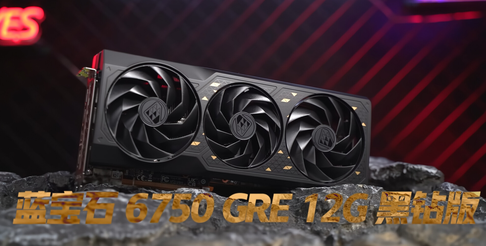
The AMD Radeon RX 6750 GRE (Golden Rabbit Edition) is a runaway success in China, where the card is found selling in volumes comparable to GeForce RTX 4060 Ti, and the likes. This is thanks to its aggressive pricing, and decent levels of performance given the maturity of drivers for the older RDNA2 graphics architecture. The RX 6750 GRE comes in two variants—a 10 GB variant with a 160-bit memory bus and 2,304 stream processors; and a 12 GB variant with the full 2,560 stream processors, similar to the globally available RX 6750 XT. For AMD, the success of the RX 6750 GRE couldn't have come at a better time, as it looks to mop up its 7 nm wafer allocation with TSMC with the "Navi 22" silicon, which went underutilized as GPU demand fell with the crypto-mining crash of 2022 and the subsequent move to the 5 nm next-generation; and so it needs these cards to sell at prices at least in line with the MSRP, of ¥2,219 (RMB) for the 10 GB variant, and ¥2,379 for the 12 GB model. Apparently some retailers are selling these cards below the MSRP, and AMD isn't liking this.

The way retail works in general, is that when an item is selling below MSRP, it encourages retailers to negotiate lower prices up the supply chain, which would inevitably cut income for AMD, and set off a feedback loop. To check exactly this, AMD rolled out a slew of measures. It will be monitoring the retail channel for retailers selling the card below MSRP, and impose a set of tiered penalties. For the first offense, a retailer will be penalized ¥500 per card sold below MSRP. For the second instance, this penalty goes up to ¥1,000 per card, and a stoppage of supply to the retailer. The RX 6750 GRE is so popular in China that it isn't just AMD's traditional AIB partners selling the SKU, but also several lesser known Chinese brands, which have purchased volumes of the RX 6750 GRE ASIC, and are belting out cards as the market demands. In related news, AMD is yet to launch the new Radeon RX 7600 XT in the Chinese market, because it doesn't want to disturb the flow of the RX 6750 GRE.

TSMC 2 nm Node to Enter Risk Production in Q4-2024, Mass Production in Q2-2025 if All Goes Well

The cutting edge 2 nm EUV foundry node by TSMC is expected to enter risk product in Q4 2024, according to a report by Taiwan-based industry observer DigiTimes. 2 nm would be an important milestone for the foundry company, as it would be the first from the company to implement GAA (gates all around) FETs, the technological successor to FinFETs, which drove silicon fabrication node development for almost a decade, from 16 nm to 3 nm. The GAAFET technology will be critical for the foundry's journey between 2 nm and 1 nm.

TSMC is expected to risk-produce chips on its 2 nm node in its new fab at the Baoshan campus in the Hsinchu Science Park, located in northern Taiwan. Should all go well with risk production, one can expect mass production of chips by Q2-2025. Until then, refinements to the company's final FinFET node, the N3 family, will remain the cutting-edge of silicon fabrication. Samsung has a similar 2025 target set for mass production on its 2 nm node, dubbed SF2. Across the Pacific, Intel Foundry Services has its Intel 20A node, which implements GAAFET (aka RibbonFET) technology aiming for similar timelines, including an ambitious 2024 mass production target.

Apple M4 & A18 Chipsets Linked to Significant Neural Engine Upgrade

Apple CEO, Tim Cook, discussed planned generative AI software features during an early February earnings call: "As we look ahead, we will continue to invest in these and other technologies that will shape the future. That includes artificial intelligence, where we continue to spend a tremendous amount of time and effort, and we're excited to share the details of our ongoing work in that space later this year." His "prepared" statement did not provide any specific insights into involved technologies, but many iPhone experts believe that the upcoming release of iOS 18 could be "the biggest update" in Apple mobile operating system history. The American multinational technology giant is seemingly taking a relaxed approach with internal artificial intelligence developments—rival smartphone maker, Samsung, has already jumped into the on-the-go AI deep end with its recently launched Galaxy S24 series. Qualcomm's Snapdragon 8 Gen 3 (for Galaxy) chipset is ready to take on all sorts of artificial intelligence-augmented tasks, while a next-gen ARM Cortex-X "Blackhawk" unit (leveraging "great" LLM performance) is in the pipeline for a late 2024 rollout.

Taiwan's Economic Daily News has reached out to insider contacts, albeit on the hardware side of things—their sources reckon that Apple is working on next generation processors that sport "significantly upgraded Neural Engine performance with additional cores." Tipsters believe that plans for 2024 include an effort to "significantly strengthen the AI computing power of the (existing) M3 and A17 processors," while the true "new generation" M4 and Bionic A18 chipsets will be augmented with greater AI computing core counts. Taiwan's top foundry is reportedly in the mix: "Apple has strengthened the AI computing performance of mobile devices and greatly increased the computing power of its own processors, which has simultaneously increased its wafer investment in TSMC. According to industry sources, Apple's wafer production volume for TSMC's 3 nm enhanced version process this year is expected to increase by more than 50% compared with last year, making it firmly the largest customer of TSMC."

ASML High-NA EUV Twinscan EXE Machines Cost $380 Million, 10-20 Units Already Booked

ASML has revealed that its cutting-edge High-NA extreme ultraviolet (EUV) chipmaking tools, called High-NA Twinscan EXE, will cost around $380 million each—over twice as much as its existing Low-NA EUV lithography systems that cost about $183 million. The company has taken 10-20 initial orders from the likes of Intel and SK Hynix and plans to manufacture 20 High-NA systems annually by 2028 to meet demand. The High-NA EUV technology represents a major breakthrough, enabling an improved 8 nm imprint resolution compared to 13 nm with current Low-NA EUV tools. This allows chipmakers to produce transistors that are nearly 1.7 times smaller, translating to a threefold increase in transistor density on chips. Attaining this level of precision is critical for manufacturing sub-3 nm chips, an industry goal for 2025-2026. It also eliminates the need for complex double patterning techniques required presently.

However, superior performance comes at a cost - literally and figuratively. The hefty $380 million price tag for each High-NA system introduces financial challenges for chipmakers. Additionally, the larger High-NA tools require completely reconfiguring chip fabrication facilities. Their halved imaging field also necessitates rethinking chip designs. As a result, adoption timelines differ across companies - Intel intends to deploy High-NA EUV at an advanced 1.8 nm (18A) node, while TSMC is taking a more conservative approach, potentially implementing it only in 2030 and not rushing the use of these lithography machines, as the company's nodes are already developing well and on time. Interestingly, the installation process of ASML's High-NA Twinscan EXE 150,000-kilogram system required 250 crates, 250 engineers, and six months to complete. So, production is as equally complex as the installation and operation of this delicate machinery.

Loongson 3A6000 CPU Reportedly Matches AMD Zen 4 and Intel Raptor Lake IPC

China's homegrown Loongson 3A6000 CPU shows promise but still needs to catch up AMD and Intel's latest offerings in real-world performance. According to benchmarks by Chinese tech reviewer Geekerwan, the 3A6000 has instructions per clock (IPC) on par with AMD's Zen 4 architecture and Intel's Raptor Lake. Using the SPEC CPU 2017 processor benchmark, Geekerwan has clocked all the CPUs at 2.5 GHs to compare the raw benchmark results to Zen 4 and Intel's Raptor Lake (Raptor Cove) processors. As a result, the Loongson 3A6000 seemingly matches the latest designs by AMD and Intel in integer results, with integer IPC measured at 4.8, while Zen 4 and Raptor Cove have 5.0 and 4.9, respectively. The floating point performance is still lagging behind a lot, though. This demonstrates that Loongson's CPU design can catching up to global leaders, but still needs further development, especially for floating point arithmetic.

However, the 3A6000 is held back by low clock speeds and limited core counts. With a maximum boost speed of just 2.5 GHz across four CPU cores, the 3A6000 cannot compete with flagship chips like AMD's 16-core Ryzen 9 7950X running at 5.7 GHz. While the 3A6000's IPC is impressive, its raw computing power is a fraction of that of leading x86 CPUs. Loongson must improve manufacturing process technology to increase clock speeds, core counts, and cache size. The 3A6000's strengths highlight Loongson's ambitions: an in-house LoongArch ISA design fabricated on 12 nm achieves competitive IPC to state-of-the-art x86 chips built on more advanced TSMC 5 nm and Intel 7 nm nodes. This shows the potential behind Loongson's engineering. Reports suggest that next-generation Loongson 3A7000 CPUs will use SMIC 7 nm, allowing higher clocks and more cores to better harness the architecture's potential. So, we expect the next generation to set a bar for China's homegrown CPU performance.

NVIDIA to Create AI Semi-custom Chip Business Unit

NVIDIA is reportedly working to set up a new business unit focused on designing semi-custom chips for some of its largest data-center customers, Reuters reports. NVIDIA dominates the AI HPC processor market, although even its biggest customers are having to shop from its general lineup of A100 series and H100 series HPC processors. There are reports of some of these customers venturing out of the NVIDIA fold, wanting to develop their own AI processor designs. It is to cater to exactly this segment that NVIDIA is setting up the new unit.

A semi-custom chip isn't just a bespoke chip designed to a customer's specifications. It is co-developed by NVIDIA and its customer, using mainly NVIDIA IP blocks, but also integrating some third-party IP blocks the customer may want; and more importantly, approach semiconductor fabrication companies such as TSMC, Samsung, or Intel Foundry Services as separate entities from NVIDIA for their wafer allocation. For example, a company like Google may have a certain amount of wafer pre-allocation with TSMC (eg: for its Tensor SoCs powering the Pixel smartphones), which it may want to tap into for a semi-custom AI HPC processor for its cloud business. NVIDIA assesses a $30 billion TAM for this specific business unit—that's all its current customers wanting to pursue their own AI processor projects, who will now be motivated to stick to NVIDIA.

TSMC & SK Hynix Reportedly Form Strategic AI Alliance, Jointly Developing HBM4

Last week SK Hynix revealed ambitious plans for its next wave of High Bandwidth Memory (HBM) products—their SEMICON Korea 2024 presentation included an announcement about cutting-edge HBM3E entering mass production within the first quarter of this year. True next-gen HBM development has already kicked off—TPU's previous report outlines an HBM4 sampling phase in 2025, followed by full production in 2026. South Korea's Pulse News believes that TSMC has been roped into a joint venture (with SK Hynix). An alleged "One Team" strategic alliance has been formed according to reports emerging from Asia—this joint effort could focus on the development of HBM4 solutions for AI fields.

Reports from last November pointed to a possible SK Hynix and NVIDIA HBM4 partnership, with TSMC involved as the designated fabricator. We are not sure if the emerging "One Team" progressive partnership will have any impact on previously agreed upon deals, but South Korean news outlets reckon that the TSMC + SK Hynix alliance will attempt to outdo Samsung's development of "new-generation AI semiconductor packaging." Team Green's upcoming roster of—"Hopper" H200 and "Blackwell" B100—AI GPUs are linked to a massive pre-paid shipment of SK Hynix HMB3E parts. HBM4 products could be fitted on a second iteration of NVIDIA's Blackwell GPU, and the mysterious "Vera Rubin" family. Notorious silicon industry tipster, kopite7kimi, believes that "R100 and GR200" GPUs are next up in Team Green's AI-cruncher queue.

Interposer and Fan-out Wafer Level Packaging Market worth $63.5 billion by 2029: MarketsandMarkets Research

The global interposer and FOWLP market is expected to be valued at USD 35.6 billion in 2024 and is projected to reach USD 63.5 billion by 2029; it is expected to grow at a CAGR of 12.3% during the forecast period according to a new report by MarketsandMarkets. The increasing demand for advanced packaging in AI and high-performance computing (HPC) are the key drivers fueling the expansion of the interposer and FOWLP market.

Interposer-based packaging is experiencing robust growth in the semiconductor industry, leveraging its ability to enhance performance and reduce power consumption by facilitating efficient connections between diverse chip components. This technology is increasingly adopted for its role in enabling high-bandwidth and high-performance applications, driving advancements in data centers, 5G infrastructure, and emerging technologies.

TSMC Allegedly Not Rushing into Adoption of High-NA EUV Machinery

DigiTimes Asia has reached out to insiders at fabrication toolmakers in an effort to delve deeper into claims made by industry analysts at the start of 2024—both SemiAnalysis and China Renaissance have proposed that TSMC is unlikely to adopt High-NA EUV production techniques within a five year period. The latest news article explores a non-upgrade approach for the next couple of years: "TSMC has not placed orders for high-numerical aperture (High-NA) extreme ultraviolet (EUV) tools and is unlikely to use the technology in 2 nm and 1.4 nm (A14) process manufacturing." Intel Foundry Services (IFS) will be one of the first semiconductor manufacturers to go online with ASML's latest and greatest machinery, although no firm timeframes have been confirmed. Team Blue's Taiwanese rival (and occasional business partner) is seemingly happy with its existing infrastructure, but industry watchdogs propose that cost considerations are key factors behind TSMC's cautious planning for the next decade.

The DigiTimes insider sources believe that TSMC will not budge until at least 2029, possibly coinciding with a 1 nm production node—analysts at China Renaissance reckon that High-NA EUV machines could be delivered in the future when facilities are readied for an "A10" codenamed process. TSMC published a very ambitious "transistor count" product timeline in early January (see below)—the first "1 nm" products are supposedly targeted for a 2030 rollout, but this schedule could change due to unforeseen circumstances. Intel is expected to "phase in" its fanciest ASML gear collection once the 18A process becomes old hat—Tom's Hardware thinks that 2026 - 2027 is a feasible timeframe.

Samsung Lands Significant 2 nm AI Chip Order from Unnamed Hyperscaler

This week in its earnings call, Samsung announced that its foundry business has received a significant order for a two nanometer AI chips, marking a major win for its advanced fabrication technology. The unnamed customer has contracted Samsung to produce AI accelerators using its upcoming 2 nm process node, which promises significant gains in performance and efficiency over today's leading-edge chips. Along with the AI chips, the deal includes supporting HBM and advanced packaging - indicating a large-scale and complex project. Industry sources speculate the order may be from a major hyperscaler like Google, Microsoft, or Alibaba, who are aggressively expanding their AI capabilities. Competition for AI chip contracts has heated up as the field becomes crucial for data centers, autonomous vehicles, and other emerging applications. Samsung said demand recovery in 2023 across smartphones, PCs and enterprise hardware will fuel growth for its broader foundry business. It's forging ahead with 3 nm production while eyeing 2 nm for launch around 2025.

Compared to its 3 nm process, 2 nm aims to increase power efficiency by 25% and boost performance by 12% while reducing chip area by 5%. The new order provides validation for Samsung's billion-dollar investments in next-generation manufacturing. It also bolsters Samsung's position against Taiwan-based TSMC, which holds a large portion of the foundry market share. TSMC landed Apple as its first 2 nm customer, while Intel announced 5G infrastructure chip orders from Ericsson and Faraday Technology using its "Intel 18A" node. With rivals securing major customers, Samsung is aggressively pricing 2 nm to attract clients. Reports indicate Qualcomm may shift some flagship mobile chips to Samsung's foundry at the 2 nm node, so if the yields are good, the node has a great potential to attract customers.

TSMC JASM Set to Expand in Kumamoto Japan

TSM, Sony Semiconductor Solutions Corporation ("SSS"), DENSO Corporation ("DENSO") and Toyota Motor Corporation ("Toyota") today announced further investment into Japan Advanced Semiconductor Manufacturing, Inc. ("JASM"), TSMC's majority-owned manufacturing subsidiary in Kumamoto Prefecture, Japan, to build a second fab, which is scheduled to begin operation by the end of the 2027 calendar year. Toyota will also take a minority stake. Together with JASM's first fab, which is scheduled to begin operation in 2024, the overall investment in JASM will exceed US$20 billion with strong support from the Japanese government.

In response to rising customer demand, JASM plans to commence construction of its second fab by the end of 2024. The increased production scale is also expected to improve overall cost structure and supply chain efficiency for JASM. With both fabs, JASM's Kumamoto site is expected to offer a total production capacity of more than 100,000 12-inch wafers per month starting from 40, 22/28, 12/16 and 6/7 nanometer process technologies for automotive, industrial, consumer and HPC-related applications. The capacity plan may be further adjusted based upon customer demand. With both fabs, the Kumamoto site is expected to directly create more than 3,400 high-tech professional jobs.
Return to Keyword Browsing
May 21st, 2024 18:56 EDT change timezone

New Forum Posts

Popular Reviews

Controversial News Posts