News Posts matching #TSMC

Return to Keyword Browsing

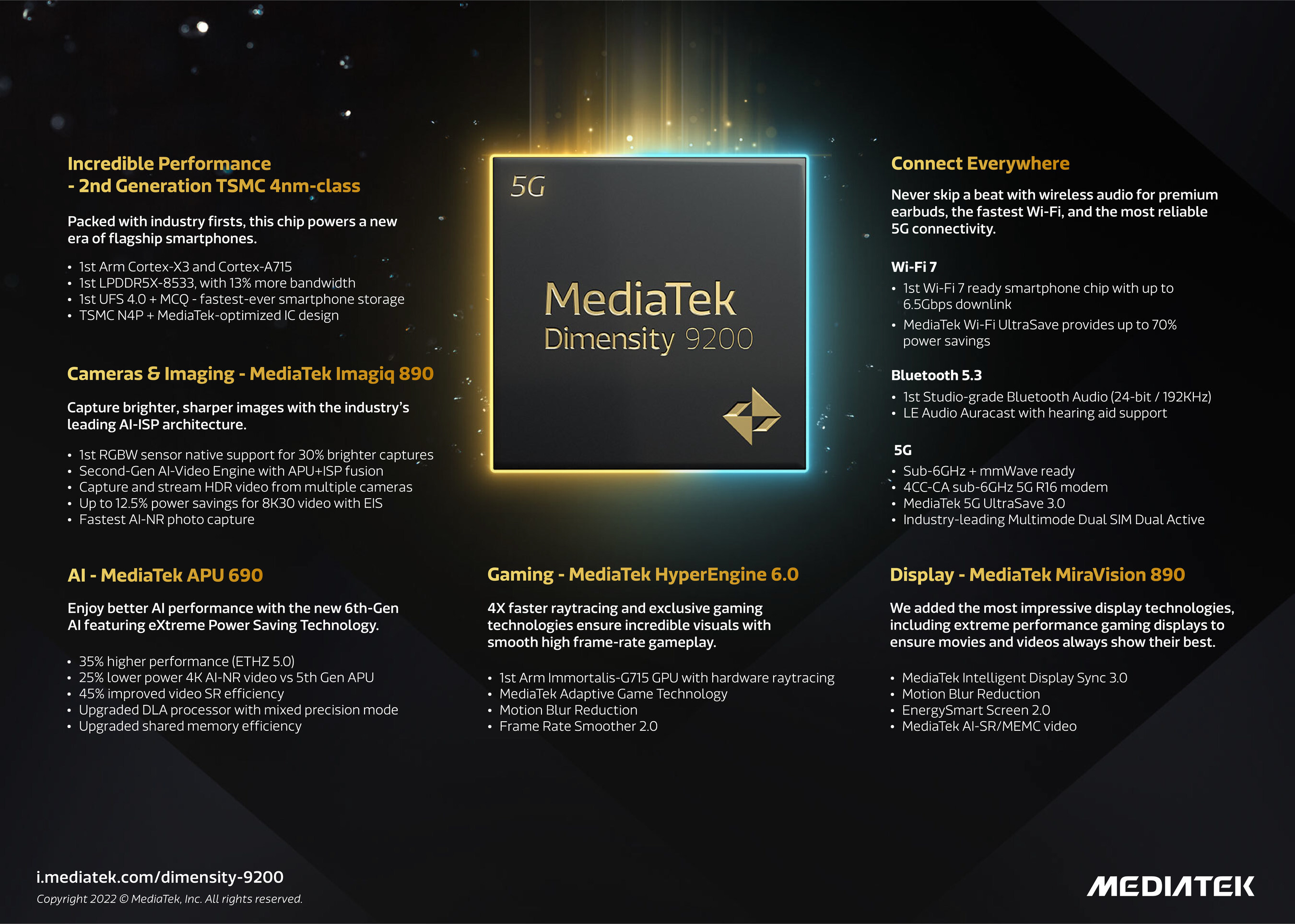
Intel Meteor Lake to Feature 50% Increase in Efficiency, 2X Faster iGPU

Intel's upcoming Meteor Lake processor family is supposedly looking good with the new performance/efficiency targets. According to the @OneRaichu Twitter account, we have a potential performance estimate for the upcoming SKUs. As the latest information notes, Intel's 14th-generation Meteor Lake will feature around a 50% increase in efficiency compared to the 13th-generation Raptor Lake designs. This means that the processor can use half the power at the same performance target at Raptor Lake, increasing efficiency. Of course, the design also offers some performance improvements besides efficiency that are significant and are yet to be shown. The new Redwood Cove P-cores will be combined with the new Crestmont E-cores for maximum performance inside U/P/H configurations with 15-45 Watt power envelopes.

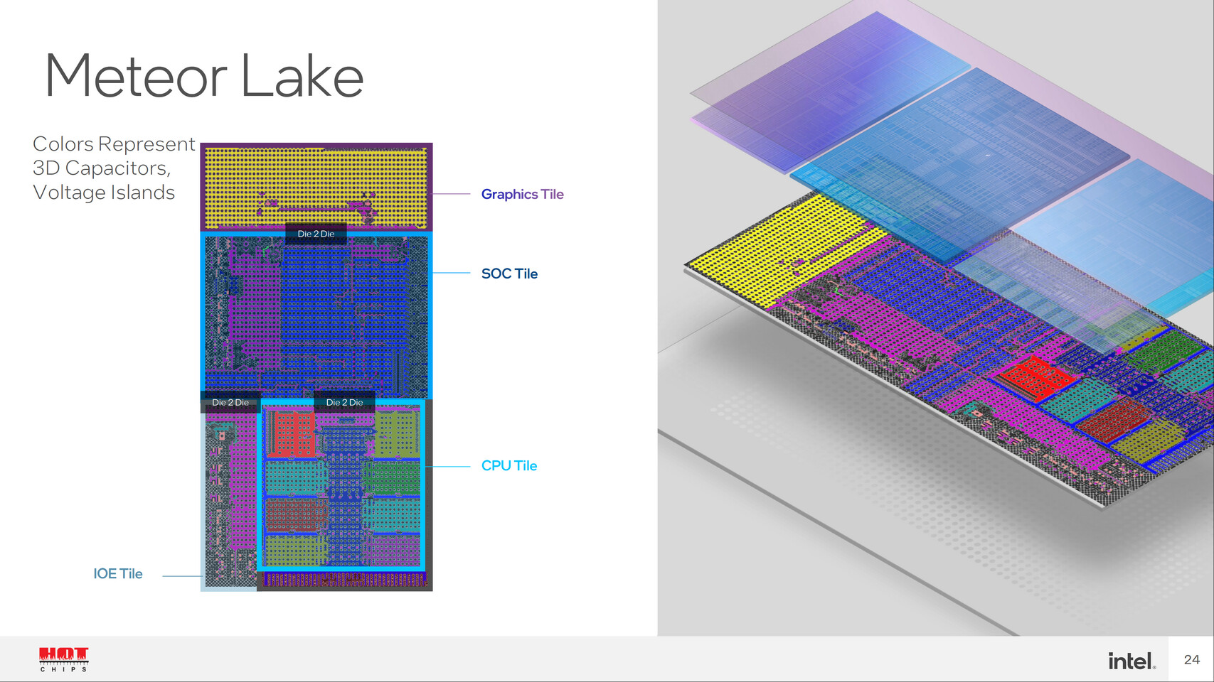
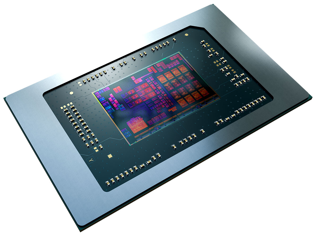
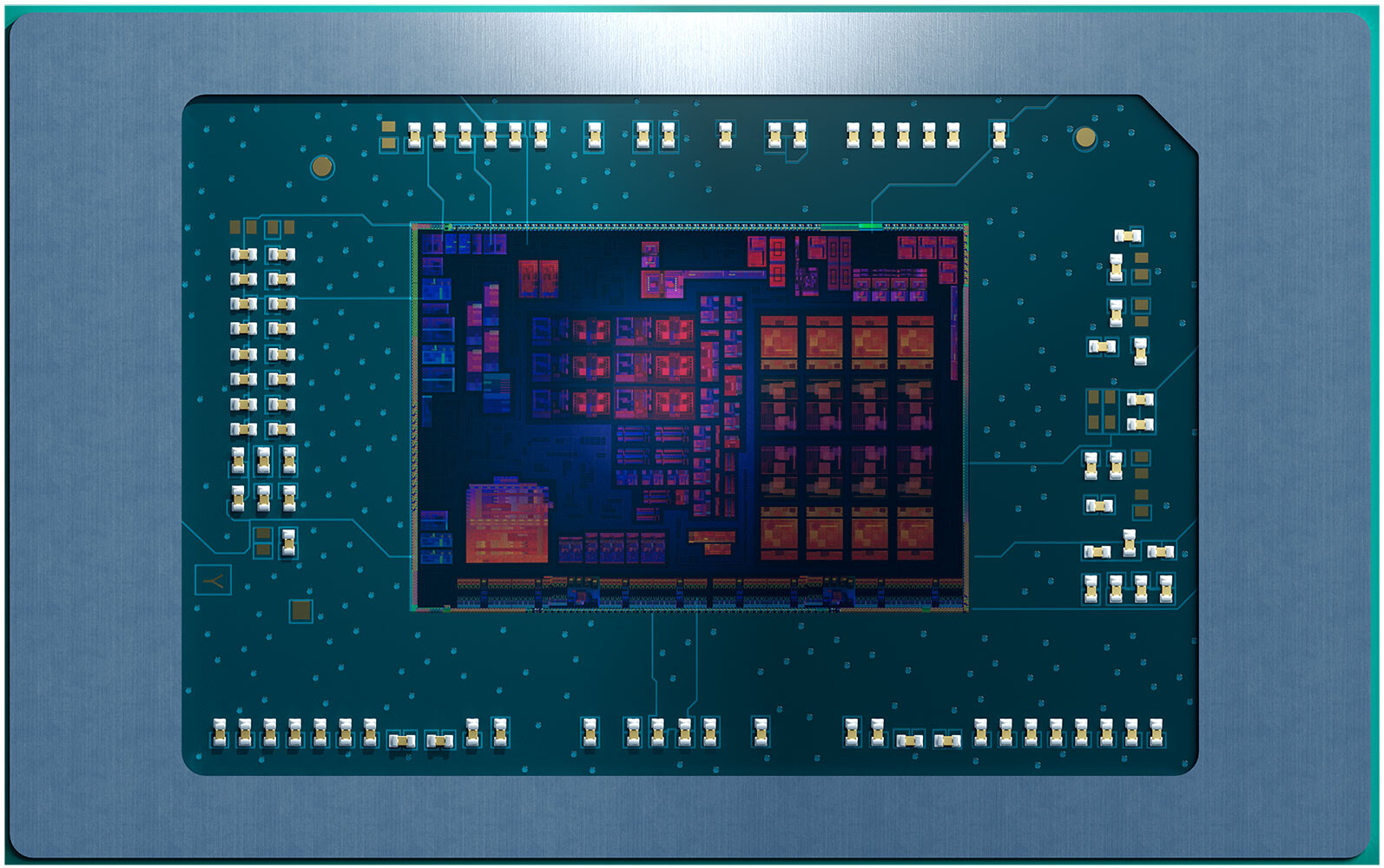
For integrated graphics, the source notes that Meteor Lake offers twice the performance of iGPU found on Raptor Lake designs. Supposedly, Meteor Lake will feature 128 EUs running 2.0+GHz compared to 96 EUs found inside Raptor Lake. The iGPU architecture will switch from Intel Iris to Xe-LPG 'Xe-MTL' family on the 14th gen models, confirming a giant leap in performance that iGPU is supposed to experience. Using the tile-based design, Intel combines the Intel 4 process for the CPU tile and the TSMC 5 nm process for the GPU tile. Intel handles final packaging for additional tuning, and you can see the separation below.

Intel Foundry Services Onboards a Fabless Customer, Deal Expected to Fetch over $4 Billion

Intel Foundry Services, the semiconductor foundry business of Intel, has onboarded an undisclosed fabless customer, the company disclosed in its Q4-2022 Financial Results presentation. This signals that the company wants to serve the semiconductor manufacturing industry beyond its own products, and scale up to demands, just like TSMC, UMC, Samsung Foundry, or other such semiconductor foundries do. The customer is looking to build chips on the Intel 3 foundry-node, which is rumored to offer performance/Watt and transistor-density figures comparable to TSMC 4N (4 nm EUV). Intel will extensively use Tower Semiconductor's silicon fabrication IP in the deal. Throughout its manufacturing lifecycle (from risk production to mass-production and completion), the deal is expected by Intel to generate over $4 billion in revenue for the company.
Image Courtesy: VideoCardz

Intel Xeon "Sapphire Rapids" to be Quickly Joined by "Emerald Rapids," "Granite Rapids," and "Sierra Forest" in the Next Two Years

Intel's server processor lineup led by the 4th Gen Xeon Scalable "Sapphire Rapids" processors face stiff competition from AMD 4th Gen EPYC "Genoa" processors that offer significantly higher multi-threaded performance per Watt on account of a higher CPU core-count. The gap is only set to widen, as AMD prepares to launch the "Bergamo" processor for cloud data-centers, with core-counts of up to 128-core/256-thread per socket. A technologically-embattled Intel is preparing quick counters as many as three new server microarchitecture launches over the next 23 months, according to Intel, in its Q4-2022 Financial Results presentation.

The 4th Gen Xeon Scalable "Sapphire Rapids," with a core-count of up to 60-core/120-thread, and various application-specific accelerators, witnessed a quiet launch earlier this month, and is shipping to Intel customers. The company says that it will be joined by the Xeon Scalable "Emerald Rapids" architecture in the second half of 2023; followed by "Granite Rapids" and "Sierra Forest" in 2024. Built on the same LGA4677 package as "Sapphire Rapids," the new "Emerald Rapids" MCM packs up to 64 "Raptor Cove" CPU cores, which support higher clock-speeds, higher memory speeds, and introduce the new Intel Trust Domain Extensions (TDX) instruction-set. The processor retains the 8-channel DDR5 memory interface, but with higher native memory speeds. The chip's main serial interface is a PCI-Express Gen 5 root-complex with 80 lanes. The processor will be built on the last foundry-level refinement of the Intel 7 node (10 nm Enhanced SuperFin); many of these refinements were introduced with the company's 13th Gen Core "Raptor Lake" client processors.

Foundry Revenue is Forecasted to Drop by 4% YoY for 2023, TrendForce Notes

TrendForce's recent analysis of the foundry market reveals that demand continues to slide for all types of mature and advanced nodes. The major IC design houses have cut wafer input for 1Q23 and will likely scale back further for 2Q23. Currently, foundries are expected to maintain a lower-than-ideal level of capacity utilization rate in the first two quarters of this year. Some nodes could experience a steeper demand drop in 2Q23 as there are still no signs of a significant rebound in wafer orders. Looking ahead to the second half of this year, orders will likely pick up for some components that underwent an inventory correction at an earlier time. However, the state of the global economy will remain the largest variable that affect demand, and the recovery of individual foundries' capacity utilization rates will not occur as quickly as expected. Taking these factors into account, TrendForce currently forecasts that global foundry revenue will drop by around 4% YoY for 2023. The projected decline for 2023 is more severe when compared with the one that was recorded for 2019.

Phison E26 Controller Powering Several Upcoming PCIe Gen 5 NVMe SSDs Detailed

At the 2023 International CES, we caught a hold of Phison, makes or arguably the most popular SSD controllers, which sprung to prominence on being the first to market with PCIe Gen 4 NVMe controllers, and now hopes to repeat it with PCIe Gen 5. We'd been shown a reference-design Phison E26-powered M.2 SSD, along with some hardware specs of the controller itself. The drive itself isn't much to look at—a standard looking M.2-2280 drive with a PCI-Express 5.0 x4 host interface, and the Phison E26 controller with its shiny IHS being prominently located next to a DDR4 memory chip, and two new-generation Micron Technology 3D NAND flash memory chips.

The Phison E26 controller, bearing the long-form model number PS5026-E26, is an NVMe 2.0 spec client-segment SSD controller. It has been built on the TSMC 12 nm FinFET silicon-fabrication node. The controller features an integrated DRAM controller with support for DDR4 and LPDDR4 memory types for use as DRAM cache. Its main flash interface is 8-channel with 32 NAND chip-enable (CE) lines, support for TLC and QLC NAND flash, a dual-CPU architecture, and hardware-acceleration for AES-256, TCG-Opal, and Pyrite. The controller features Phison's 5th generation LPDC ECC and internal RAID engines. For its reference-design 2 TB TLC-based drive, Phison claims sequential transfer rates of up to 13.5 GB/s reads, with up to 12 GB/s writes. The 4K random-access performance is rated at up to 1.5 million IOPS reads, with up to 2 million IOPS writes.

AMD Ryzen 7040 Series "Phoenix Point" Mobile Processor I/O Detailed: Lacks PCIe Gen 5

The online datasheets of some of the first AMD Ryzen 7040 series "Phoenix Point" mobile processors went live, detailing the processor's I/O feature-set. We learn that AMD has decided to give PCI-Express Gen 5 a skip with this silicon, at least in its mobile avatar. The Ryzen 7040 SoC puts out a total of 20 PCI-Express Gen 4 lanes, all of which are "usable" (i.e. don't count 4 lanes toward chipset-bus). This would mean that the silicon has a full PCI-Express 4.0 x16 interface for discrete graphics, and a PCI-Express 4.0 x4 link for a CPU-attached M.2 NVMe slot; unlike the "Raphael" desktop MCM and the "Dragon Range" mobile MCM, whose client I/O dies put out a total of 28 Gen 5 lanes (24 usable, with x16 PEG + two x4 toward CPU-attached M.2 slots).

Another interesting aspect about "Phoenix Point" is its memory controllers. The SoC features a dual-channel (four sub-channel) DDR5 memory interface, besides support for LPDDR5 and LPDDR5x. DDR5-5600 and LPDDR5-7600 are the native speeds supported. What's really interesting is the maximum amount of memory supported, which stands at 256 GB—double that of "Raphael" and "Dragon Range," which top out at 128 GB. This bodes well for the eventual Socket AM5 APUs AMD will design based on the "Phoenix Point" silicon. Older Ryzen 5000G "Cezanne" desktop APUs are known for superior memory overclocking capabilities to 5000X "Vermeer," with the monolithic nature of the silicon favoring latencies. Something similar could be expected from "Phoenix Point."

Top 10 TSMC Customers Said to have Cut Orders for 2023

On the day of TSMC's celebration of the mass production start of its 3 nm node, news out of Taiwan suggests that all of its top 10 customers have cut their orders for 2023. However, the cuts are unlikely to affect its new node, but rather its existing nodes, with the 7 and 6 nm nodes said to be hit the hardest, by as much as a 50 percent utilisation reduction in the first quarter of 2023. The 28 nm and 5 and 4 nm nodes are also said to be affected, although it's unclear by how much at this point in time.

Revenue is expected to fall by at least 15 percent in the first quarter of 2023 for TSMC, based on numbers from DigiTimes. The fact that TSMC has increased its 2023 pricing by six percent should at least help offset some of the potential losses for the company, but it all depends on the demand for the rest of the year. Demand for mobile devices is down globally, which is part of the reason why so many of TSMC's customers have cut back their orders, as Apple, Qualcomm and Mediatek all produce their mobile SoCs at TSMC. Add to this that the demand for computers and new computer components are also down, largely due to the current pricing and TSMC is in for a tough time next year.

TSMC Holds 3nm Volume Production and Capacity Expansion Ceremony, Marking a Key Milestone for Advanced Manufacturing

TSMC today held a 3 nanometer (3 nm) Volume Production and Capacity Expansion Ceremony at its Fab 18 new construction site in the Southern Taiwan Science Park (STSP), bringing together suppliers, construction partners, central and local government, the Taiwan Semiconductor Industry Association, and members of academia to witness an important milestone in the Company's advanced manufacturing.

TSMC has laid a strong foundation for 3 nm technology and capacity expansion, with Fab 18 located in the STSP serving as the Company's GIGAFAB facility producing 5 nm and 3 nm process technology. Today, TSMC announced that 3 nm technology has successfully entered volume production with good yields, and held a topping ceremony for its Fab 18 Phase 8 facility. TSMC estimates that 3 nm technology will create end products with a market value of US$1.5 trillion within five years of volume production.

TSMC to Mark 3 nm Mass Production Start, Looking at Potential New Fabs in Japan and Germany

According to news out of Taiwan, TSMC will hold a ceremony to mark the official mass production start of its 3 nm node on the 29th of December. This is said to help "shatter doubts about de-Taiwanization" or in simpler terms, that Taiwan will lose its golden goose as TSMC invests abroad. The 3 nm fab—known as fab 18—is based in southern Taiwan's Tainan and the ceremony also marks the start of an expansion of TSMC's most advanced fab. TSMC is said to be kicking off its N3E node production sometime in the second half of 2023, followed by its N3P node in 2024, all of which should take place at fab 18, which also produces 5 nm wafers.

In related news, according to Reuters, a Japanese lawmaker from the ruling party has said that TSMC is considering a second plant in Japan, in addition to its current joint venture that is already under construction. TSMC's response to Reuters was that the company isn't ruling out Japan for future fabs, but that the company doesn't have any current plans. At the same time, TSMC is said to be sending executives to Dresden, Germany in early 2023, for a second round of talks about building a fab to help support the European auto industry, although this would be a 28/22 nm fab, which is far from cutting edge these days, although a lot more advanced than most fabs making chips for the auto industry.

Global Top 10 Foundries' Total Revenue Grew by 6% QoQ for 3Q22, but Foundry Industry's Revenue Performance Will Enter Correction Period in 4Q22

According to TrendForce's research, the total revenue of the global top 10 foundries rose by 6% QoQ to US$35.21 billion for 3Q22 as the release of the new iPhone series during the second half of the year generated significant stock-up activities across Apple's supply chain. However, the global economy shows weak performances, and factors such as China's policy on containing COVID-19 outbreaks and high inflation continue to impact consumer confidence. As a result, peak-season demand in the second half of the year has been underwhelming, and inventory consumption is proceeding slower than anticipated. This situation has led to substantial downward corrections to foundry orders as well. For 4Q22, TrendForce forecasts that the total revenue of the global top 10 foundries will register a QoQ decline, thereby terminating the boom of the past two years—when there was an uninterrupted trend of QoQ revenue growth.

Regarding individual foundries' performances in 3Q22, the group of the top five was led by TSMC, followed by Samsung, UMC, GlobalFoundries, and SMIC. Their collective global market share (in revenue terms) came to 89.6%. Most foundries were directly impacted by clients slowing down their stock-up activities or significantly correcting down their orders. Only TSMC was able to make a notable gain due to Apple's strong stock-up demand for the SoCs deployed in this year's new iPhone models. TSMC saw its revenue rise by 11.1% QoQ to US$20.16 billion, and the corresponding market share expanded to 56.1%. The growth was mainly attributed to the ≤7 nm nodes, whose share in the foundry's revenue had kept climbing and reached 54% in the third quarter. Conversely, Samsung actually experienced a slight QoQ drop of 0.1% in foundry revenue even though it had also benefited from the component demand related to the new iPhone series. Partially impacted by the weakening of the Korean won, Samsung's market share fell to 15.5%.

TSMC Announces Updates for TSMC Arizona

TSMC today announced that in addition to TSMC Arizona's first fab, which is scheduled to begin production of N4 process technology in 2024, TSMC has also started the construction of a second fab which is scheduled to begin production of 3 nm process technology in 2026. The overall investment for these two fabs will be approximately US$40 billion, representing the largest foreign direct investment in Arizona history and one of the largest foreign direct investments in the history of the United States.

In addition to the over 10,000 construction workers who helped with construction of the site, TSMC Arizona's two fabs are expected to create an additional 10,000 high-paying high-tech jobs, including 4,500 direct TSMC jobs. When complete, TSMC Arizona's two fabs will manufacture over 600,000 wafers per year, with estimated end-product value of more than US $40 billion.

Apple and NVIDIA First Customers of TSMC's Arizona Fab

Apple and NVIDIA will be among the first customers of TSMC's swanky new $12 billion semiconductor fab in Arizona, USA. Apple will be the first major player to kick off mass-production in the fab, and will be closely followed by NVIDIA. Both companies plan to produce some of their inventory in Arizona, and ramp proportionately up as the fab grows in capacity.

The plan with TSMC's Arizona fab was to originally make 5 nm and 4 nm EUV chips, with an output of 20,000 wafers a month, but the company now expects to deploy a more advanced node to keep up with what will be considered cutting-edge when the fab goes live (think 2 nm-class); and also double the output to 40,000 wafers a month. The capacity should ensure Apple and NVIDIA make their most cutting-edge chips on the node (away from Asia), so there could be tighter export controls, and build supply-chain resilience in the face of security problems arising in the Taiwan straits.

Alleged Apple M2 Max Performance Figures Show Almost 20% Single-Core Improvement

Apple's ongoing pursuit of leading performance in custom silicon packages continues with each new generation of Apple Silicon. Today, we have alleged Geekbench performance figures of the upcoming M2 Max chip, designed for the upcoming Mac devices. Featuring the same configuration with two E-cores and eight P-cores, the chip is rumored to utilize TSMC's 3 nm design. However, that is yet to be confirmed by Apple, so we don't have the exact information. In the GB5 single-thread test, the CPU set a single-core performance target of 1899 points, while the multi-core score was 8737. While last year's M1 Max chips can reach 1787 single-core and 12826 multi-core scores, these configurations are benchmarked in a Mac Studio, which has better cooling and allows for higher clocks to be achieved.

Apples to apples (pun intended) comparison with the M1 Max chip inside of a MacBook Pro version with presumably the same cooling capacity, which gets 1497 single-core and 11506 multi-core score, the new M2 Max chip is 19.4% faster in single-core results. Multi-core improvements should follow, and this M2 Max result should be different from the final product. We await more benchmarks to confirm this performance increase and the correct semiconductor manufacturing node.

NVIDIA to Relocate Logistics Center From Hong Kong to Taiwan

According to news out of Taiwan, NVIDIA is getting ready to move its logistics center from Hong Kong to Taiwan. The information comes from Taiwan's Minister of Economic Affairs, Wang Mei-Hua, so the source should be fairly reliable. The Taiwanese government has apparently been in negotiation with NVIDIA since some time last year and the two have now reached a consensus.

The media report didn't mention where NVIDIA will locate its new logistics center, but the company and the Taiwanese government have been discussing tax subsidies to help facilitate the move. Wang told the local media that the new logistics center should boost the local industry, least not because NVIDIA is already working with TSMC, as well as many other local suppliers and manufacturers. No details were given on when the move would take place, but it's likely to be a transition that will be drawn out, due to the fact that NVIDIA is still going to have to supply all of its customers during the move.

TSMC 3 nm Wafer Pricing to Reach $20,000; Next-Gen CPUs/GPUs to be More Expensive

Semiconductor manufacturing is a significant investment that requires long lead times and constant improvement. According to the latest DigiTimes report, the pricing of a 3 nm wafer is expected to reach $20,000, which is a 25% increase in price over a 5 nm wafer. For 7 nm, TSMC managed to produce it for "just" $10,000; for 5 nm, it costs the company to make it for the $16,000 mark. And finally, the latest and greatest technology will get an even higher price point at $20,000, a new record in wafer pricing. Since TSMC has a proven track record of delivering constant innovation, clients are expected to remain on the latest tech purchasing spree.

Companies like Apple, AMD, and NVIDIA are known for securing orders for the latest semiconductor manufacturing node capacities. With a 25% increase in wafer pricing, we can expect the next-generation hardware to be even more expensive. Chip manufacturing price is a significant price-determining factor for many products, so the 3 nm edition of CPUs, GPUs, etc., will get the highest difference.

TSMC's Morris Chang Says Arizona Fab Will Produce 3 nm Chips in the Future

Although Morris Chang is no longer in charge of the day to day business at TSMC, the founder of the company is still getting his hands dirty. Chang attended the APEC Economic Leaders Meeting last week, as part of Taiwan's delegation and was questioned by the media about TSMC's future plans. The specific question was about TSMC's Arizona fab, which will initially produce chips using a 5 nm node. The US$12 billion plant is scheduled to kick off production at some point in 2024, by which time the 5 nm node should be a commonly used node rather than close to cutting edge.

When questioned about the future of the Arizona fab, Morris Chang answered that it will be moving to a 3 nm node, which is currently TSMC's most cutting edge node, that has gone into volume production earlier this year with th N3 node, which is set to be followed by the N3E node. According to Chang, there's interest by several countries to have TSMC set up fabs there, but apparently this is not something TSMC is considering at the moment. One potential reason for this would be a suitable labour force, something that has already proven to be tough for the Arizona fab.

Taiwan Reportedly Preparing a Domestic Version of CHIPS Act, To Reveal More Details on Thursday

Suppose you are following the inside of the semiconductor industry. In that case, you must be aware of the United States CHIPs act, where the US government plans to invest billions of dollars into domestic companies to boost the production of semiconductors devices on American soil. However, it seems like the Biden administration isn't the only governing body that realizes the importance of making semiconductors that power everything from entertainment to government, as Taiwan is supposed to announce a similar act for Taiwanese semiconductor makers like TSMC, MediaTek, GlobalWafers, UMC, etc. to simulate additional manufacturing and development on Taiwanese soil.

On Thursday, the Taiwanese government is expected to announce a 25% tax cut for research and development efforts of companies manufacturing their chips on the domestic playground. In addition to this tax deduction, Taiwan also plans to impose an additional 5% tax break on equipment purchasing, so companies like TSMC and GlobalWafers that purchase leading-edge equipment will be enjoying a healthy 30% smaller tax bill. This money is a Taiwanese way of creating additional funds for R&D purposes so these companies can bolster their CapEx with additional funds. We await to see what will happen tomorrow and update this story with more information as the official act gets announced.

Eliyan Closes $40M Series A Funding Round and Unveils Industry's Highest Performance Chiplet Interconnect Technologies

Eliyan Corporation, credited for the invention of the semiconductor industry's highest-performance and most efficient chiplet interconnect, today announced two major milestones in the commercialization of its technology for multi-die chiplet integration: the close of its Series A $40M funding round, and the successful tapeout of its technology on an industry standard 5-nanometer (nm) process.

Eliyan's NuLink PHY and NuGear technologies address the critical need for a commercially viable approach to enabling high performance and cost-effectiveness in the connection of homogeneous and heterogenous architectures on a standard, organic chip substrate. It has proven to achieve similar bandwidth, power efficiency, and latency as die-to-die implementations using advanced packaging technologies, but without the other drawbacks of specialized approaches.

MediaTek Launches Flagship Dimensity 9200 Chipset for Incredible Performance and Unmatched Power Saving

MediaTek today launched the Dimensity 9200, its latest 5G chipset powering the next era of flagship smartphones. Boasting extreme performance and intelligent power efficiency, the new SoC brings immersive all-day gaming experiences, ultra-sharp image capturing and support for both mmWave 5G and sub-6 GHz connectivity to consumers around the globe.

"MediaTek's Dimensity 9200 combines ultimate performance with significant power savings, extending battery life and keeping smartphones cool," said JC Hsu, Corporate Vice President and General Manager of MediaTek's wireless communications business unit at MediaTek. "With notably brighter image capturing and improved gaming speeds, along with the latest display enhancements, the Dimensity 9200 will bring new possibilities for next-gen smartphones that come in a variety of stylish and foldable form factors."

Chinese Chip Makers are Trying to Circumvent US Sanctions by Slowing Down Chip Performance

In what can only be called an unusual move, several Chinese fabless chip makers—such as Alibaba and Biren Technology—who manufacturers at TSMC, are looking at running their chips slower. The reason for this is that they're trying to circumvent the US sanctions against Chinese chip makers. It should be noted that these are chips that have already taped out and gone into sample production, such as Biren's BR100 GPU.As reported earlier today, Alibaba even had one of its chips delisted from the official SPEC ranking, due to being unavailable and it's possible that it's one of the chips that's affected by the US sanctions.

Considering that the Chinese chip makers are dependent on the same cutting edge nodes at TSMC as the likes of Nvidia, AMD, Qualcomm etc. it would potentially lead to more capacity for these companies at TSMC. According to the report by the Financial Times, Biren has had to stop shipments of its GPUs, as the company is going to have to prove that its chips don't violate the US export control restrictions. Apparently the rules to work out if a chip falls under the US sanctions or not are anything but clear. One metric is apparently based on the bidirectional transfer rate, which is capped at below 600 GB/s between chips, but the tricky part is that this metric can be calculated in several different ways. As such, Biren has dropped the transfer rate from 640 to 576 GB/s according to the Financial Times. The sanctions are likely to cause longer term concerns for TSMC as well, as the company is likely to lose several big customers for its cutting edge nodes, at least for the time being.

AMD Navi 31 RDNA3 GPU Pictured

Here's the first picture of the "Navi 31" GPU at the heart of AMD's fastest next-generation graphics cards. Based on the RDNA3 graphics architecture, this will mark an ambitious attempt by AMD to build the first multi-chip module (MCM) client GPU featuring more than one logic die. MCM GPUs aren't new in the enterprise space with Intel's "Ponte Vecchio," but this would be the first such GPU meant for hardcore gaming graphics products. AMD had made MCM GPUs in the past, but those have been packages with just one logic die, surrounded by memory stacks. "Navi 31" is an MCM of as many as eight logic dies, and no memory stacks (no, those aren't HBM stacks in the picture below).

It's rumored that "Navi 31" features one or two SIMD chiplets dubbed GCDs, featuring the GPU's main number crunching machinery, the RDNA3 compute units. These chiplets are likely built on the most advanced silicon fabrication node, likely TSMC 5 nm EUV, but we'll see. The GDDR6 memory controllers handling the chip's 384-bit wide GDDR6 memory interface, will be located on separate chiplets built on a slightly older node, such as TSMC 6 nm. This is not multi-GPU-a-stick, because both SIMD chiplets have uniform access to the entire 384-bit wide memory bus (which is not 2x 192-bit but 1x 384-bit), besides the other ancillaries. The "Navi 31" MCM are expected to be surrounded by JEDEC-standard 20 Gbps GDDR6 memory chips.

One of TSMC's Biggest Customers Cuts 3nm Wafer Orders As Consumer Demand Deflates

A major unnamed customer of TSMC has reportedly cut their order for 3 nm wafers. Foundry customers usually place orders for cutting-edge foundry nodes several quarters in advance, in exchange for priority foundry allocations, and preferential rates, while foundries use revenues from these orders to develop the capacity for manufacture these chips. The 3 nm customer could be anyone—Qualcomm, Mediatek, NVIDIA, AMD, or Intel. Order cancellations have reportedly had a domino-effect on the upstream supply-chain of TSMC, hitting suppliers of raw materials, manufacturing equipment, and other consumables. There is an industry-wide slump in demand for consumer electronics and PC hardware, which reflects in the slump in revenues and/or guidance in quarterly financial results releases by prominent companies.

TSMC N1 Node Chip Plant Said to be Under Planning

Based on news out of Taiwan, TSMC is said to be in the early planning stages of yet another chip plant, this time for its first N1 node. The new plant will reportedly be built in a science park in Taoyuan, less than an hour south west of Taipei, according to the Commercial Times. TSMC already has a pair of chip packaging and testing facilities in the science park, making it a suitable location for a chip plant. This will be TSMC's most northern chip manufacturing plant in Taiwan, although it's not expected to start pilot production until sometime in 2027. TSMC hasn't confirmed any of the details, but the company didn't outright deny the report either.

Despite the potential global downturn in the economy, TSMC appears to be fully committed to continue to build new fabs for increasingly smaller nodes. The company is set to start its first commercial production on its N3 node this quarter and is expecting the N3 node to contribute as much as four to six percent of its overall revenue in 2023. Its N2 node should enter commercial production in 2025, but not much is known about the state of the N2 node at this point in time. The N1 node might end up being a 1.4 nm node, based on TSMC's measurements, but the company is still in the very beginning of the R&D phase for this node.

TSMC Launches OIP 3DFabric Alliance to Shape the Future of Semiconductor and System Innovations

TSMC today announced the Open Innovation Platform (OIP) 3DFabric Alliance at the 2022 Open Innovation Platform Ecosystem Forum. The new TSMC 3DFabric Alliance is TSMC's sixth OIP Alliance and the first of its kind in the semiconductor industry that joins forces with partners to accelerate 3D IC ecosystem innovation and readiness, with a full spectrum of best-in-class solutions and services for semiconductor design, memory modules, substrate technology, testing, manufacturing, and packaging. This alliance will help customers achieve speedy implementation of silicon and system-level innovations and enable next-generation HPC and mobile applications using TSMC's 3DFabric technologies, a comprehensive family of 3D silicon stacking and advanced packaging technologies.

"3D silicon stacking and advanced packaging technologies open the door to a new era of chip-level and system-level innovation, and also require extensive ecosystem collaboration to help designers navigate the best path through the myriad options and approaches available to them," said Dr. L.C. Lu, TSMC fellow and vice president of design and technology platform. "Through the collective leadership of TSMC and our ecosystem partners, our 3DFabric Alliance offers customers an easy and flexible way to unlocking the power of 3D IC in their designs, and we can't wait to see the innovations they can create with our 3DFabric technologies."

Alphawave IP Achieves Its First Testchip Tapeout for TSMC N3E Process

Alphawave IP (LSE: AWE), a global leader in high-speed connectivity for the world's technology infrastructure, today announced the successful tapeout of its ZeusCORE100 1-112 Gbps NRZ/PAM4 Serialiser-Deserialiser ("SerDes"), Alphawave's first testchip on TSMC's most advanced N3E process. Alphawave IP will be exhibiting this new product alongside its complete portfolio of high-performance IP, chiplet, and custom silicon solutions at the TSMC OIP Forum on October 26 in Santa Clara, CA as the Platinum sponsor.

ZeusCORE100 is Alphawave's most advanced multi-standard-SerDes, supporting extra-long channels over 45dB and the most requested standards such as 800G Ethernet, OIF 112G-CEI, PCIe GEN6, and CXL 3.0. Attendees will be able to visit the Alphawave booth and meet the company's technology experts including members of the recently acquired OpenFive team. OpenFive is a longstanding partner of TSMC through the OIP Value Chain Aggregator (VCA) program. OpenFive is one of a select few companies with an idea-to-silicon methodology in TSMC's latest technologies, and advanced packaging capabilities, enabling access to the most advanced foundry solution available with the best Power-Performance-Area (PPA). With Alphawave's industry-leading IP portfolio and the addition of OpenFive's capabilities, designers can create systems on a chip (SoCs) that pack more compute power into smaller form factors for networking, AI, storage, and high-performance computing (HPC) applications.
Return to Keyword Browsing
May 21st, 2024 20:53 EDT change timezone

New Forum Posts

Popular Reviews

Controversial News Posts