News Posts matching #Zen 4c

Return to Keyword Browsing

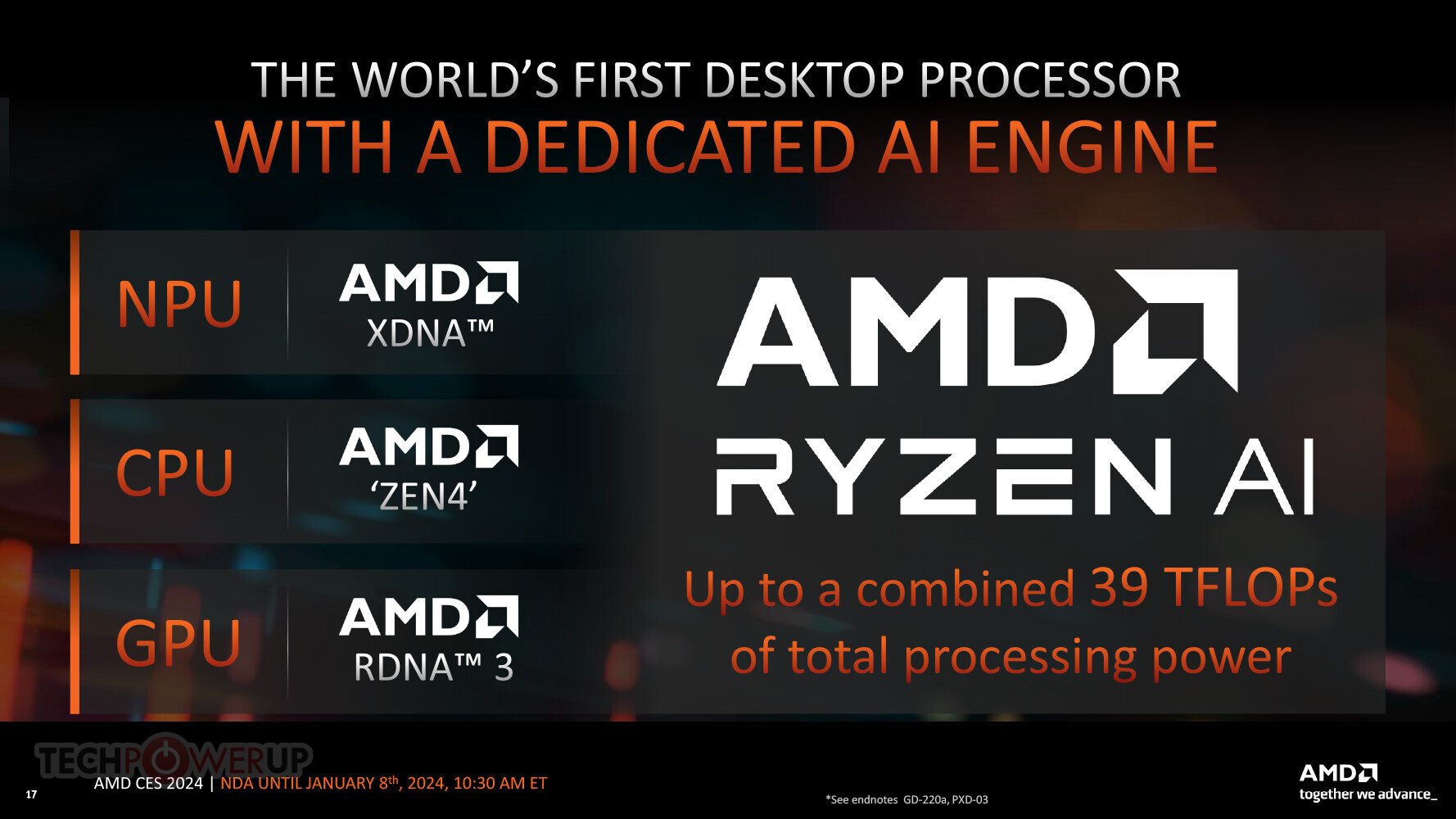
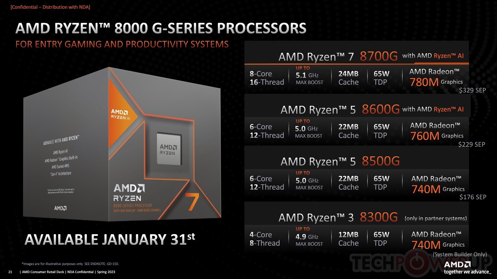
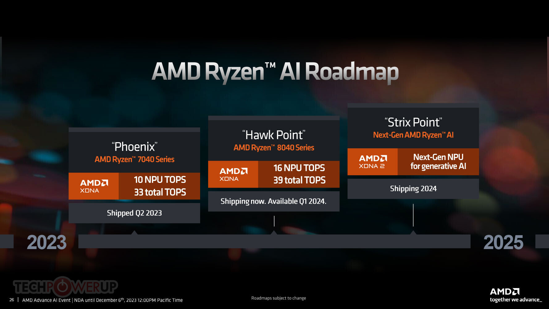
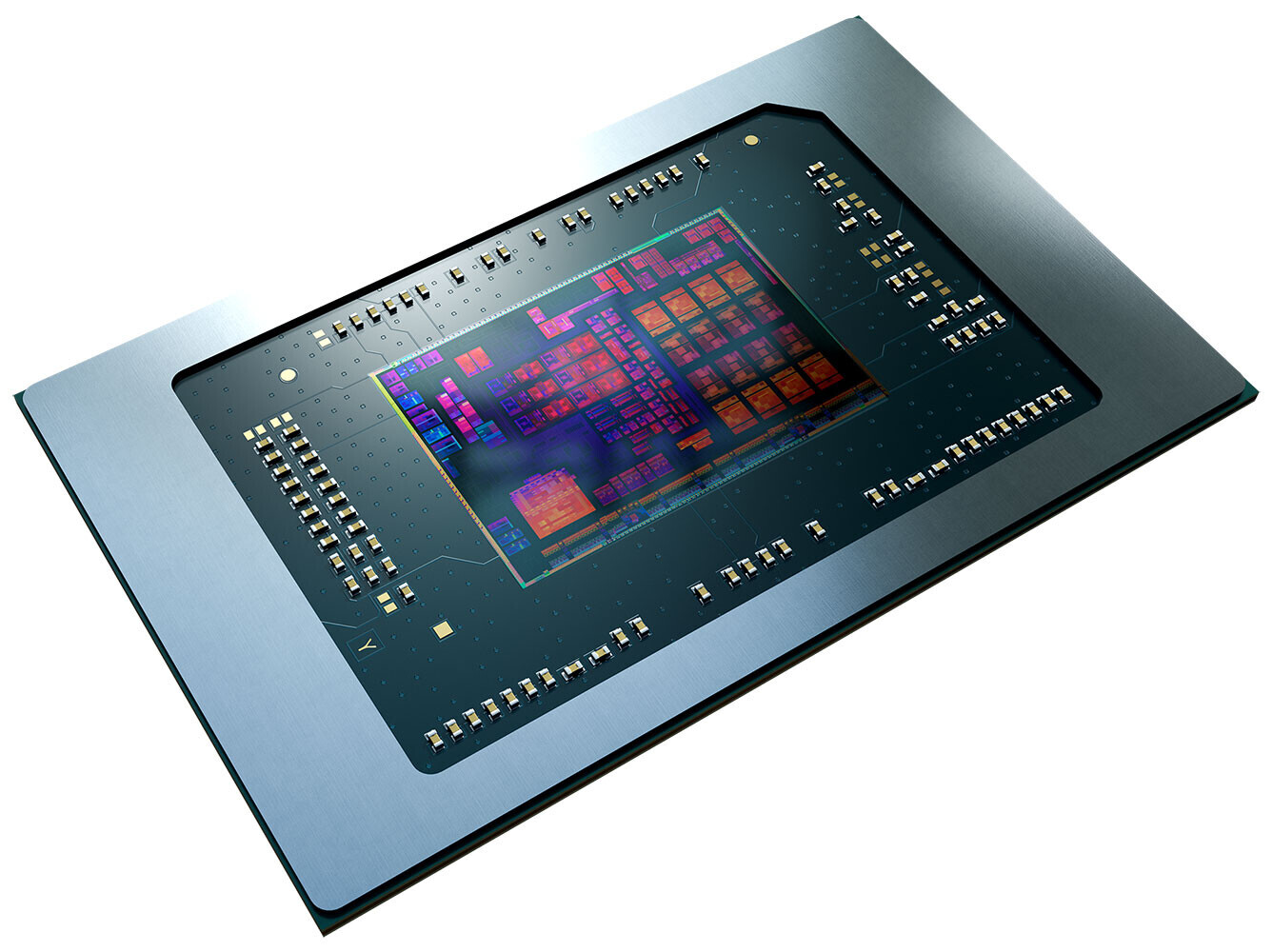
AMD Readies Ryzen 7 8700F and Ryzen 5 8400F for Retail Channel Launch

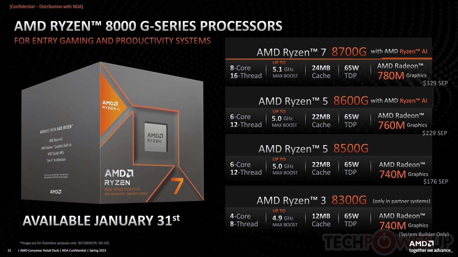
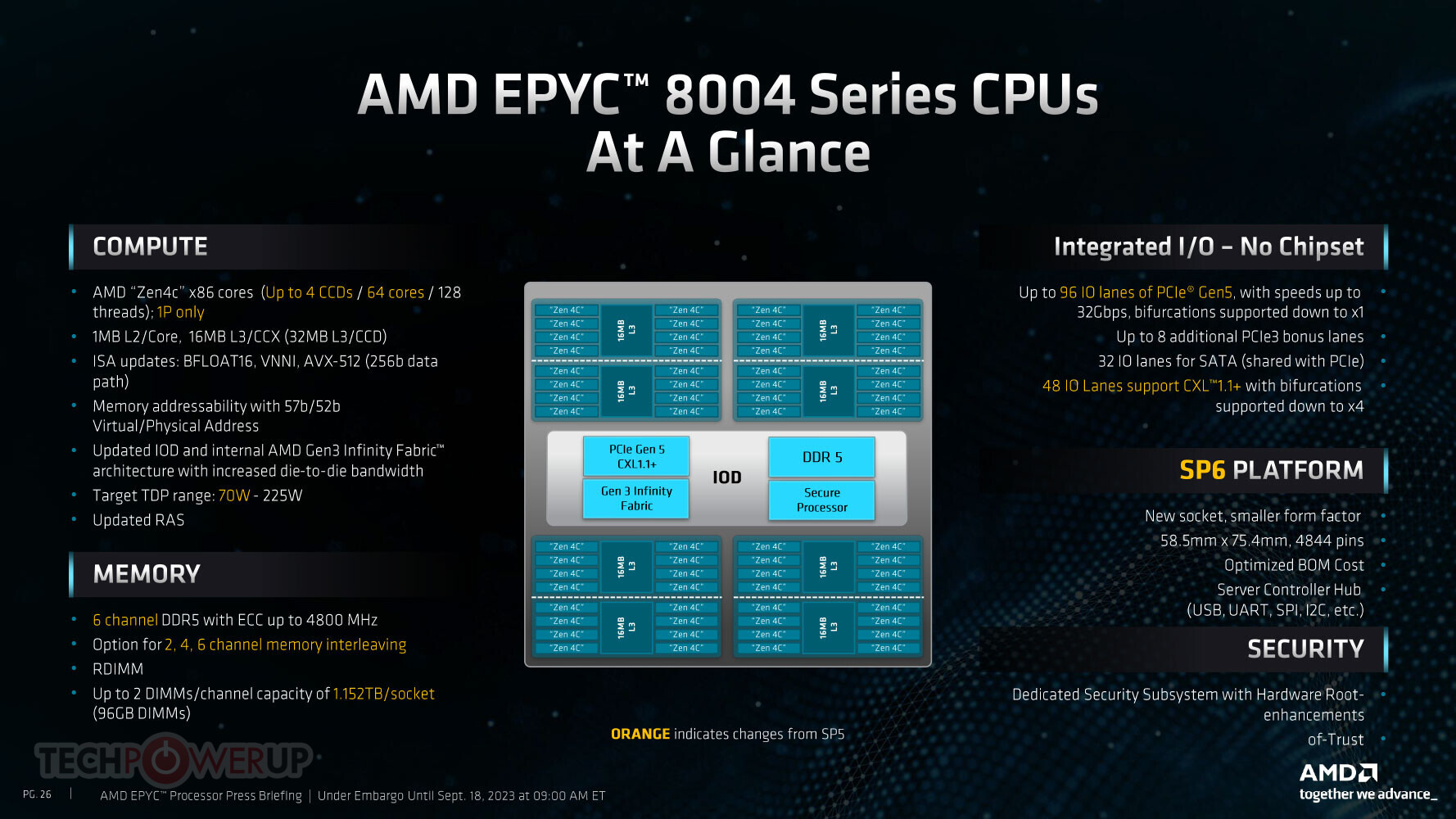
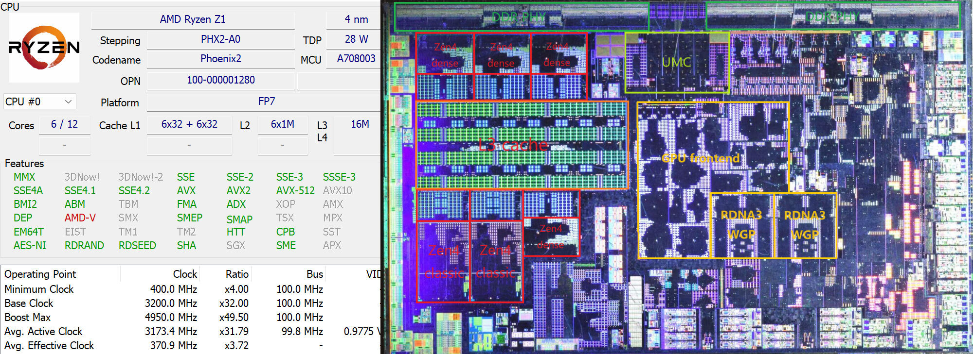
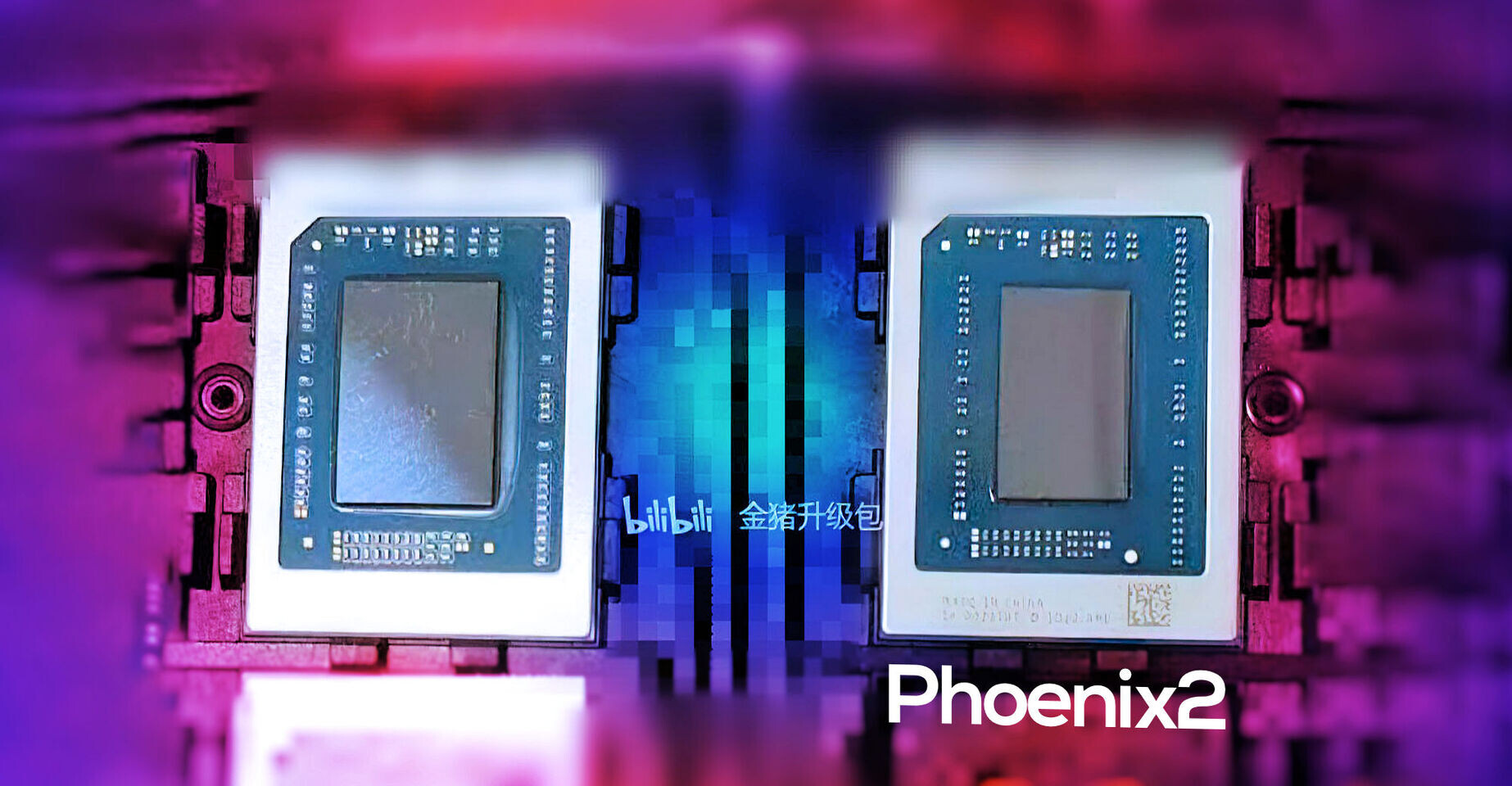
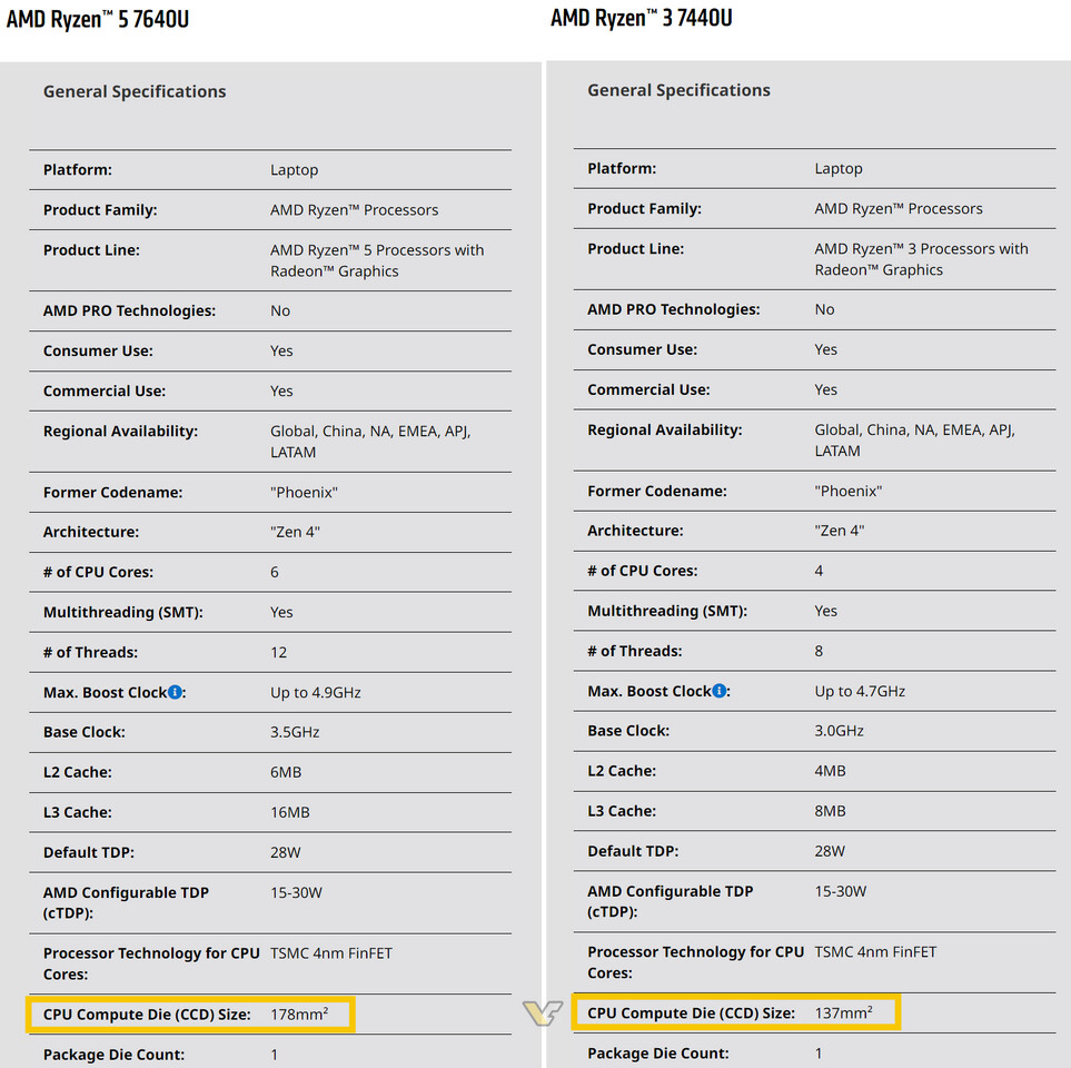
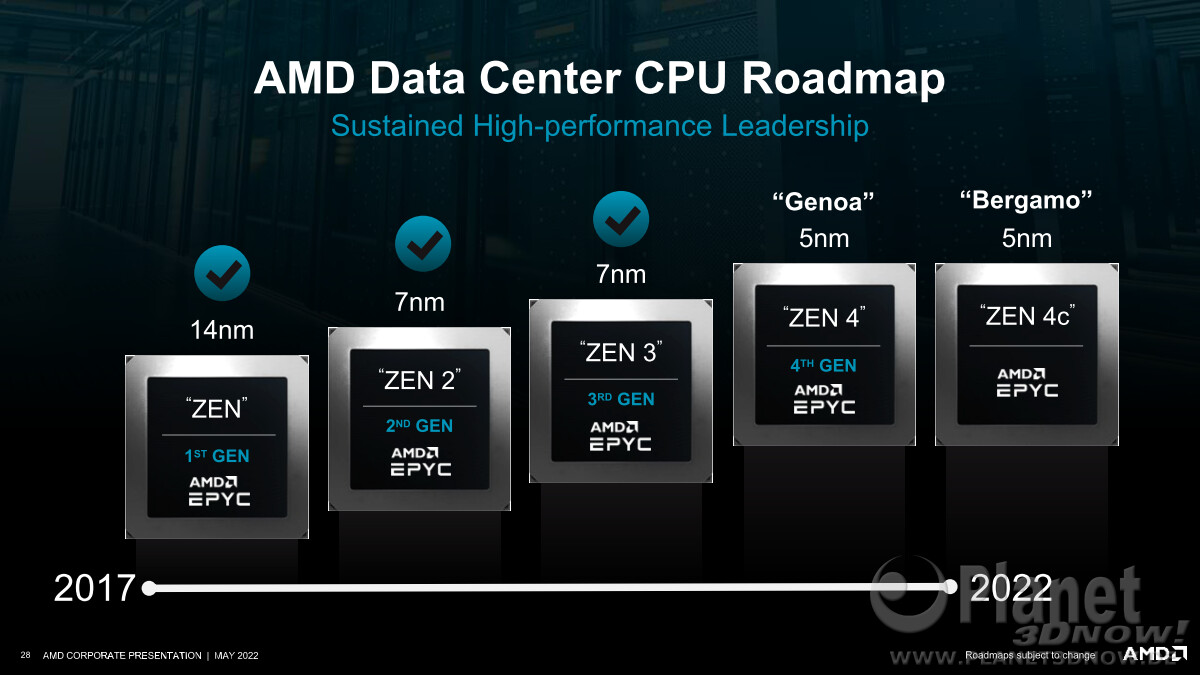
AMD is reportedly planning to launch the Ryzen 7 8700F and Ryzen 5 8400F Socket AM5 desktop processors for a global launch, in the retail channel, as boxed processors. The two chips had launched earlier this month in the Chinese retail market. The 8700F reportedly comes with an OPN of 100-100001590BOX, while the 8400F is marked 100-100001591BOX. The "F" in both SKUs denotes a lack of integrated graphics. The Ryzen 7 8700F is an 8-core/16-thread processor based on the 4 nm "Hawk Point" silicon, while the 8400F is a 6-core/12-thread processor based on "Phoenix 2," which offers two "Zen 4" cores that run at higher clock speeds, and four "Zen 4c" cores that run at lower speeds.

The lack of an iGPU isn't the only thing differentiating the 8700F from the 8700G, the new chip even comes with slightly lower CPU clock speeds—100 MHz lower base and maximum boost frequencies. The 8700F CPU runs at a base frequency of 4.10 GHz, with 5.00 GHz maximum boost, when compared to the 4.20/5.10 GHz speeds of the 8700G. The 8400F, on the other hand, runs at 4.20 GHz base frequency, and a 4.70 GHz maximum boost frequency that applies to at least its two "Zen 4" cores; its four "Zen 4c" cores run at lower frequencies. There is no word on pricing. One reason you could want an 8700F over something like a 7700 would be its appetite for memory overclocking, if you can overlook the lack of integrated graphics, a smaller L3 cache, and most importantly, the lack of PCIe Gen 5, and four fewer PCIe lanes.

AEWIN Introduces SCB Network Appliances Powered by AMD EPYC 8004

AEWIN provides a series of performant Network Appliances and Edge Server powered by single AMD Zen 4c EPYC 8004 processor codenamed Siena. The latest AMD Siena CPU is produced with 5 nm manufacturing technology to have up to 64 cores (extreme density of 2CCX/CCD) and 225 W TDP with lower energy consumption compared to EPYC SP5. Siena SP6 CPU has the best performance per watt and is with the support of rich I/O and CXL 1.1.

SCB-1945 (1U) and SCB-1947A (2U) are two performant Network Appliances supporting 12x DDR5 sockets and 4x/8x PCIe Gen 5 slots for AEWIN self-design NICs with 1G to 100G copper/fiber interfaces (with/without bypass function) or other accelerators and NVMe SSDs. Both models provide the flexibility to change 2x front panel PCIe slots to 1x PCIe x16 slot for installing off-the-shelf add-on card for additional functions required. It can support 400G NIC card installed such as NVIDIA Mellanox PCIe 5.0 NIC.

AMD Zen 5 Details Emerge with GCC "Znver5" Patch: New AVX Instructions, Larger Pipelines

AMD's upcoming family of Ryzen 9000 series of processors on the AM5 platform will carry a new silicon SKU under the hood—Zen 5. The latest revision of AMD's x86-64 microarchitecture will feature a few interesting improvements over its current Zen 4 that it is replacing, targeting the rumored 10-15% IPC improvement. Thanks to the latest set of patches for GNU Compiler Collection (GCC), we have the patch set that proposes changes taking place with "znver5" enablement. One of the most interesting additions to the Zen 5 over the previous Zen 4 is the expansion of the AVX instruction set, mainly new AVX and AVX-512 instructions: AVX-VNNI, MOVDIRI, MOVDIR64B, AVX512VP2INTERSECT, and PREFETCHI.

AVX-VNNI is a 256-bit vector version of the AVX-512 VNNI instruction set that accelerates neural network inferencing workloads. AVX-VNNI delivers the same VNNI instruction set for CPUs that support 256-bit vectors but lack full 512-bit AVX-512 capabilities. AVX-VNNI effectively extends useful VNNI instructions for AI acceleration down to 256-bit vectors, making the technology more efficient. While narrow in scope (no opmasking and extra vector register access compared to AVX-512 VNNI), AVX-VNNI is crucial in spreading VNNI inferencing speedups to real-world CPUs and applications. The new AVX-512 VP2INTERSECT instruction is also making it in Zen 5, as noted above, which has been present only in Intel Tiger Lake processor generation, and is now considered deprecated for Intel SKUs. We don't know the rationale behind this inclusion, but AMD sure had a use case for it.

The Zen 4c Cores in the Ryzen 8000G APUs are Clocked Slower than the Zen 4 Cores

AMD has revealed the full specs of its upcoming Ryzen 8000G APUs and it turns out that the Zen 4c cores aren't clocking as high as the Zen 4 cores in the Ryzen 5 8500G and Ryzen 3 8300G. We should point out that the 8300G has a singular Zen 4 core and three Zen 4c Cores here, so there's no confusion. The Zen 4 cores in the 8500G have a base clock of 4.1 GHz, while the 8300G comes in at 4.0 GHz, with both of the APU's Zen 4c cores having a base clock of 3.2 GHz. Oddly enough, AMD lists the overall base clock of the 8500G as 3.5 GHz and the 8300G as 3.4 GHz with a notice that reads "Represents the average effective base frequency of all cores." AMD is in other words averaging the clock speeds of the two different cores to come up with an approximate base clock.

The Zen 4 cores in the 8500G boost up to 5 GHz, with the 8300G boosting to 4.9 GHz, whereas the Zen 4c cores in the 8500G boost up to 3.7 GHz and in the 8300G to 3.6 GHz. Here AMD doesn't provide an estimated frequency equivalent. Despite being budget models in the Ryzen 8000G-series of APUs, both SKUs get two USB4 ports with full 40 Gbps capabilities, plus a pair of USB 3.2 Gen 2 (10 Gbps) ports. Furthermore the Radeon 740M GPU will be clocked at 2.8 GHz in both APUs, but both SKUs are limited to a mere four graphics cores, whereas the Ryzen 5 8600G gets eight at the same clock speed and the Ryzen 7 8700G gets 12 at 2.9 GHz. All four APUs also support DisplayPort 2.1.

AMD's Phoenix 1 and Phoenix 2 APUs Differ in PCIe Lane Count, Affects NVMe Drive Performance and GPU PCIe Lane Count

At CES, AMD didn't give away too many technical details of its upcoming Ryzen 8000G-series APUs, but details are starting to trickle out and it's not all good news. As has been known for some time, AMD is using two different chips to make the Ryzen 8000G APUs and they're known as the Phoenix 1 and Phoenix 2, where the Phoenix 2 parts feature Zen 4c cores, which are not present in the Phoenix 1 APUs. This in and of itself shouldn't be a huge issue, although the Zen 4c CPU cores can be slightly slower in some tasks based on testing of AMD's EPYC server parts.

However, PCGamesN noticed that Gigabyte has posted the full specs for the B650E Aorus Elite X AX Ice motherboard and it looks like there's a much bigger difference between the Phoenix 1 and Phoenix 2 based APUs. Namely, the Phoenix 2 APUs have fewer PCIe lanes and as such are limited to two PCIe 4.0 lanes for the secondary NVMe slot. As if this wasn't bad enough, the Phoenix 2 APUs only have four PCIe 4.0 lanes for add-in GPUs, whereas the Phoenix 1 APUs have eight. This is very likely to lead to reduced performance if a higher-end GPU is used with such an APU. Note that this will vary depending on the motherboard design, but many B650/B650E boards feature a similar design with regards to the PCIe lanes coming from the CPU socket. Luckily, it's easy to avoid this issue, as the Ryzen 5 8600G and the Ryzen 7 8700G are both Phoenix 1 designs, whereas the Ryzen 5 8500G is the only Phoenix 2 design available in retail, as the Ryzen 3 8300G is an OEM only part.

AMD Announces Ryzen 8000G Series Desktop APUs, Select Models Feature Ryzen AI

AMD today announced the Ryzen 8000G line of desktop APUs. These come in the Socket AM5 package, and are supported by all motherboards based on the AMD X670/E, B650/E, and A620 chipsets, with some requiring UEFI firmware updates. Since USB BIOS Flashback is standard issue on AMD motherboards, this should be no problem. With Ryzen 7000 series "Raphael" desktop processors that debut the "Zen 4" microarchitecture, AMD had standardized integrated graphics, however, the iGPU for these are just enough for desktop/productivity workloads, offering comparable performance to the iGPUs of Intel 13th Gen Core desktop processors. AMD doesn't consider Ryzen 7000 chips as APUs for this reason. An APU has to be a processor with powerful integrated graphics that can offer entry-level gaming, high-res content consumption, or multi-monitor productivity, and "Raphael" isn't it. Enter the Ryzen 8000G series.

The AMD Ryzen 8000G series debuts four APU models, the Ryzen 7 8700G, the Ryzen 5 8600G, the Ryzen 5 8500G, and the Ryzen 3 8300G. The 8700G and 8600G are based on the 4 nm "Hawk Point" silicon, feature Ryzen AI, and are the first desktop processors to feature an NPU (neural processing unit). The 8500G and 8300G are based on the 4 nm "Phoenix 2" silicon. The Ryzen 7 8700G leads the pack, and is a maxed out implementation of "Hawk Point," featuring an 8-core/16-thread CPU based on the "Zen 4" microarchitecture, the full Radeon 780M integrated graphics implementation with 12 RDNA3 compute units; and the Ryzen AI XDNA NPU. The processor has a combined AI throughput of 39 TOPS, with 16 TOPS from the NPU. For reference, an Intel Core Ultra 7 165H "Meteor Lake" mobile processor with its AI Boost NPU, has a combined AI throughput of 34 TOPS.

GIGABYTE Releases AGESA 1.1.0.1a AM5 Motherboard BIOS Updates, Suggests 8700G Based on "Hawk Point," Not "Phoenix"

GIGABYTE released UEFI firmware (BIOS) updates for its Socket AM5 motherboards encapsulating the AMD AGESA ComboAM5 PI 1.1.0.1a microcode. This latest version of AGESA has sparked speculation that some of AMD's upcoming Ryzen 8000G desktop APUs are in fact based on the newer "Hawk Point" silicon, and not "Phoenix." AMD released its Ryzen 8040 series "Hawk Point" mobile processors earlier this month, with a faster NPU that results in an up to 40% increase in AI interference performance over that of "Phoenix." "Hawk Point" is essentially identical to "Phoenix," including its first generation XDNA architecture based NPU, however the NPU's clock speed has been dialed up. If AMD is building some of its Ryzen 8000G desktop APU models on "Hawk Point" instead of "Phoenix," then we have our first solid hint that AMD is bringing Ryzen AI to the desktop platform, and that the Ryzen 8000G will end up being the first desktop processors with an NPU.

AMD is expected to be building at least two APU models based on the "Hawk Point" silicon, the Ryzen 7 8700G, and the Ryzen 5 8600G. The lower models, namely the 8500G and Ryzen 3 8300G, are expected to be based on the smaller "Phoenix 2" silicon, with a hybrid CPU that combines two "Zen 4" cores with up to four "Zen 4c" cores. The "Zen 4c" cores may feature an identical instruction set architecture (ISA) and IPC to the regular "Zen 4" cores, but have tighter Vcore limits, and operate at lower clock speeds. This makes the two available "Zen 4" cores the de facto "performance" cores, and AMD flags them as UEFI CPPC "preferred cores," ensuring the OS guides a bulk of its processing traffic to them. Both "Phoenix" and "Hawk Point" feature an identical CPU setup, with up to eight "Zen 4" cores.

AMD 5th Gen EPYC "Turin" Pictured: Who Needs Accelerators When You Have 192 Cores?

AMD's upcoming server processor, the 5th Gen EPYC "Turin," has been pictured as an engineering sample is probably being evaluated by the company's data-center or cloud customers. The processor has a mammoth core-count of 192-core/384-thread in its high-density cloud-focused variant that uses "Zen 5c" CPU cores. Its regular version that uses larger "Zen 5" cores that can sustain higher clock speeds, also comes with a fairly high core-count of 128-core/256-thread, up from the 96-core/192-thread of the "Zen 4" based EPYC "Genoa."

The EPYC "Turin" server processor based on "Zen 5" comes with an updated sIOD (server I/O die), surrounded by as many as 16 CCDs (CPU complex dies). AMD is expected to build these CCDs on the TSMC N4P foundry node, which is a more advanced version of the TSMC N4 node the company currently uses for its "Phoenix" client processors, and the TSMC N5 node it uses for its "Zen 4" CCD. TSMC claims that the N4P node offers an up to 22% improvement in power efficiency over N5, as well as a 6% increase in transistor density. Each of the "Zen 5" CCDs is confirmed to have 8 CPU cores sharing 32 MB L3 cache memory. A total of 16 such CCDs add up to the processor's 128-core/256-thread number. The high-density "Turin" meant for cloud data-centers, is a whole different beast.

AMD Ryzen 8000G Socket AM5 Desktop APU Lineup Detailed

Here is our first look at the higher end of AMD's Ryzen 8000G series Socket AM5 desktop APU lineup. The company is planning to bring its 4 nm "Phoenix" and "Phoenix 2" monolithic silicon to the socketed desktop platform, to cover two distinct markets. Models based on the larger "Phoenix" silicon cater to the market that wants a sufficiently powerful CPU, but with a powerful iGPU that's fit for entry-level gaming, or graphics-intensive productivity tasks; whereas the smaller "Phoenix 2" silicon ties up the lower end of AMD's AM5 desktop processor stack, as it probably has a lower bill of materials than a "Raphael" multi-chip module.

The lineup is led by the Ryzen 7 8700G, a direct successor to the Ryzen 7 5700G "Cezanne." This chip gets the full 8-core/16-thread "Zen 4" CPU, along with its 16 MB shared L3 cache; and the full featured Radeon 780M iGPU with its 12 compute units worth 768 stream processors. The CPU features a maximum boost frequency of 4.20 GHz. This is followed by the Ryzen 5 8600G, which is based on the same "Phoenix" silicon as the 8700G, but with 6 out of 8 "Zen 4" cores enabled, and a maximum CPU boost frequency of 4.35 GHz, and the 16 MB L3 cache left untouched. It's likely that the Radeon 780M is unchanged from the 8700G.
Update 13:59 UTC: A CPU-Z screenshot of the Ryzen 7 8700G surfaced, which confirms that it features the maxed out Radeon 780M iGPU

Intel "Sierra Forest" Xeon System Surfaces, Fails in Comparison to AMD Bergamo

Intel's upcoming Sierra Forest Xeon server chip has debuted on Geekbench 6, showcasing its potential in multi-core performance. Slated for release in the first half of 2024, Sierra Forest is equipped with up to 288 Efficiency cores, positioning it to compete with AMD's Zen 4c Bergamo server CPUs and other ARM-based server chips like those from Ampere for the favor of cloud service providers (CSP). In the Geekbench 6 benchmark, a dual-socket configuration featuring two 144-core Sierra Forest CPUs was tested. The benchmark revealed a notable multi-core score of 7,770, surpassing most dual-socket systems powered by Intel's high-end Xeon Platinum 8480+, which typically scores between 6,500 and 7,500. However, Sierra Forest's single-core score of 855 points was considerably lower, not even reaching half of that of the 8480+, which manages 1,897 points.

The difference in single-core performance is a matter of choice, as Sierra Forest uses Crestmont-derived Sierra Glen E-cores, which are more power and area-efficient, unlike the Golden Cove P-cores in the Sapphire Rapids-based 8480+. This design choice is particularly advantageous for server environments where high-core counts are crucial, as CSPs usually partition their instances by the number of CPU cores. However, compared to AMD's Bergamo CPUs, which use Zen 4c cores, Sierra Forest lacks pure computing performance, especially in multi-core. The Sierra Forest lacks hyperthreading, while Bergaamo offers SMT with 256 threads on the 128-core SKU. Comparing the Geekbench 6 scores to AMD Bergamo EPYC 9754 and Sierra Forest results look a lot less impressive. Bergamo scored 1,597 points in single-core, almost double that of Sierra Forest, and 16,455 points in the multi-core benchmarks, which is more than double. This is a significant advantage of the Zen 4c core, which cuts down on caches instead of being an entirely different core, as Intel does with its P and E-cores. However, these are just preliminary numbers; we must wait for real-world benchmarks to see the actual performance.

AMD Readies Even More Derivatives of the 4 nm "Phoenix" Processor Silicon

AMD's "Phoenix" monolithic processor silicon drives the company's Ryzen 7040 series mobile processor lineup, and possible some of its upcoming Ryzen 7000G desktop processor models. It is the first chip from the AMD camp to feature an AI accelerator, besides up to 8 "Zen 4" CPU cores, and a large iGPU based on the latest RDNA3 graphics architecture, with up to 12 compute units, the latest display I/O and media acceleration capabilities. Over the course of its lifecycle, AMD realized that it can't use the nearly 200 mm² silicon built on the expensive 4 nm node to power lower-end processor SKUs, and so developed the smaller 137 mm² "Phoenix 2" silicon that lacks the AI accelerator, has a smaller iGPU with just 4 compute units, and a unique hybrid CPU with 2 "Zen 4" and 4 "Zen 4c" cores. We're now hearing that the company is designing even more derivatives.

The PCI ID Repository discovered two new IDs believed to reference the iGPU models of "Phoenix 3" and "Phoenix 4" chips. At this point we have no clue what the two chips could be, and what the mixture of their CPU, iGPU, and AI accelerator components could be, especially given that AMD is able to carve out Ryzen 3 SKUs from "Phoenix 2." We speculate that "Phoenix 3" and "Phoenix 4" could reference rebranding such as "Escher," although it could even be entirely new chips with different combinations of "Zen 4" and "Zen 4c" cores.

ASRock Begins Rolling Out AGESA 1.1.0.0 Firmware with Phoenix APU Support

ASRock began rolling out UEFI firmware updates for its Socket AM5 motherboards that encapsulate AMD AGESA 1.1.0.0 ComboAM5PI microcode. This would be the second release of AGESA to support AMD's upcoming Ryzen 7000G "Phoenix" and "Phoenix 2" desktop APUs that the company reportedly plans to launch later this year. The AGESA 1.1.0.0 microcode comes with the SMU version 76.72.0 for "Phoenix" and "Phoenix 2," and continues with version 84.79.223 for "Raphael" and "Raphael-X" processors.

Unlike several past generations of Ryzen branded desktop APUs that only had 2-3 processor models in the retail channel, AMD is reportedly planning a slightly bigger lineup of APUs for the Socket AM5 platform, consisting of Ryzen 3, Ryzen 5, and possibly Ryzen 7 processor models, and their Ryzen PRO variants. The Ryzen 3 and Ryzen 5 models are expected to be based on the "Phoenix 2" silicon that has a combination of two "Zen 4" and four "Zen 4c" CPU cores and an iGPU with 4 compute units; while it is rumored that at least one Ryzen 5 and Ryzen 7 processor model will be built on "Phoenix," which has up to eight "Zen 4" cores, and a large iGPU with up to 12 compute units. So far we haven't seen reports of AMD bringing Ryzen AI to the desktop platform.

AMD Introduces Ryzen 5 and Ryzen 3 Mobile Processors with "Zen 4c" Cores

AMD today launched its first client processors that feature the compact "Zen 4c" CPU cores, with the Ryzen 5 7545U and Ryzen 3 7440U mobile processors for thin-and-light notebooks. The "Zen 4c" CPU core is a compacted version of the "Zen 4" core without the subtraction of any hardware components, but rather a high density arrangement of them on the 4 nm silicon. A "Zen 4c" core is around 35% smaller in area on the die than a regular "Zen 4" core. Since none of its components is removed, the core features an identical IPC (single thread performance) to "Zen 4," as well as an identical ISA (instruction set). "Zen 4c" also supports SMT or 2 threads per core. The trade-off here is that "Zen 4c" cores are generally clocked lower than "Zen 4" cores, as they can operate at lower core voltages. This doesn't, however, make the "Zen 4c" comparable to an E-core by Intel's definition, these cores are still part of the same CPU clock speed band as the "Zen 4" cores, at least in the processors that's being launched today.

The Ryzen 5 7545U and Ryzen 3 7440U mobile processors formally debut the new 4 nm "Phoenix 2" monolithic silicon. This chip is AMD's first hybrid processor, in that it has a mixture of two regular "Zen 4" cores, and four compact "Zen 4c" cores. The six cores share an impressive 16 MB of L3 cache. All six cores feature 1 MB of dedicated L2 cache. There is no complex hardware-based scheduler involved, but a software based solution that's deployed by AMD's Chipset Software, which tells the Windows scheduler to see the "Zen 4" cores as UEFI CPPC "preferred cores," and prioritize traffic to them, as they can hold on to higher boost frequency bins. The "Phoenix 2" silicon inherits much of the on-die power-management feature-set from the "Phoenix" and "Rembrandt" chips, and so are capable of a high degree of power savings with underutilized CPU cores and iGPU compute units.

AMD EPYC 8004 "Siena" Processors with "Zen 4c" and New SP6 Platform Announced

AMD today rolled out the new compacted Socket SP6 server platform designed for smaller servers locally deployed at the edge by organizations. With CPU core-counts of up to 64-core/128-thread, these processors are based on the "Zen 4c" microarchitecture, which comes with identical IPC and ISA to "Zen 4," but with smaller L3 cache available per core. The EPYC 8004 series targets traditional data-centers located on-site for organizations. Even if the heavy-lifting of the IT for them is performed by remote data-centers or cloud providers, organizations still need smaller edge server deployments. The EPYC 8004 series caters to a different kind of servers than the ones the lower core-count models of EPYC 9004 "Genoa" do.

With the EPYC 8004 series, AMD is debuting a new smaller CPU socket called SP6. The socket measures 58.5 mm x 75.4 mm, compared to the 76.0 mm x 80.0 mm of Socket SP5 powering EPYC 9004 "Genoa" and EPYC 97x4 "Bergamo." Socket SP5 is an LGA with a pin count of 4,844, compared to SP5, which is LGA-6096. The first line of processors for this socket, the EPYC 8004 series, are codenamed "Siena." These are very much part of the 4th Gen EPYC series, a lineage it shares with "Genoa" for data-center servers, "Genoa-X" for compute servers, and "Bergamo" for high-density cloud.

AMD Ryzen Z1 APU Utilizes Zen 4c Cores - Discovered by Reviewer in China

A die-shot of AMD's 4 nm "Phoenix 2" monolithic APU emerged over the weekend—possibly the first example of a Team Red hybrid core processor, utilizing a combination of bog standard Zen 4 cores as well as "compacted" Zen 4c units. Phoenix 2 has been hiding in plain sight it seems, within Ryzen Z1 series APUs—that have much in common with mobile/laptop-oriented 7040U products. David Huang has posted an analysis of a Ryzen Z1 APU via his review as posted on Zhuanlan, where he investigates the intriguing combination of Zen 4 and Zen 4c cores.

As interpreted/translated by Tom's Hardware: "HWiNFO, a system information, monitoring, and diagnostics utility, confirms that the Ryzen Z1, codenamed Phoenix 2, is on the PHX2-A0 stepping. It differs from AMD's Ryzen 7040U series (Phoenix) with the PHX-A1 stepping. The Ryzen Z1 has been rumored to be a clone of the Ryzen 5 7540U for a long time now." Laptops housing the latter APU are reported to have reached retail markets in certain territories, while the Ryzen Z1 (non-Extreme) SoC has not debuted in any new devices. A cheaper ASUS ROG Ally is expected to arrive in the near future with the lesser chip.

Die-shot Suggests "Phoenix 2" is AMD's First Hybrid Processor

The 4 nm "Phoenix 2" monolithic APU silicon powering the lower end of AMD's Ryzen 7040-series mobile processors, could very well be the company's first hybrid core processor, even though the company doesn't advertise it as such. We first caught whiff of "Phoenix 2" back in July, when it was described as being a physically smaller chip than the regular "Phoenix." It was known to have just 6 CPU cores, and a smaller iGPU with 4 RDNA3 compute units; in comparison to the 8 CPU cores and 12 compute units of the "Phoenix" silicon. At the time a lack of 2 CPU cores and 8 CUs were known to be behind the significant reduction in die size from 178 mm² to 137 mm², but it turns out that there's a lot more to "Phoenix 2."

A die shot of "Phoenix 2" emerged on Chinese social media platform QQ, which reveals two distinct kinds of CPU cores. There are six cores in all, but two of them appear larger than the other four. The obvious inference here, is that the larger cores are "Zen 4," and the smaller ones are the compacted "Zen 4c." The "Zen 4c" core has the same core machinery as "Zen 4," albeit it is re-arranged to favor lower area on the die. The trade-off here is that the "Zen 4c" core operates at lower voltages and lower clock-speeds than the regular "Zen 4" cores. At the same clock speeds, both kinds of cores have an identical IPC. The two also have an identical ISA, so any software threads migrating between the cores will not encounter runtime errors. Unlike Intel Thread Director, AMD can use a less sophisticated software-based solution to ensure that the right kind of workload is allocated to the right kind of cores, and prevent undesirable migration between the two kinds of cores. Unlike the hardware-based Thread Director, AMD's solution can be continually updated.

AMD Confirms Ryzen 3 7440U Will Feature Hybrid Phoenix2 APU

Talking with XDA-Developers, AMD has confirmed more details about the upcoming Phoenix2 APU, which should debut with Ryzen 3 7440U and Ryzen 5 7540U APUs. Unlike the larger Phoenix APU, the Phoenix2 APU will have a hybrid design with Zen 4 and Zen 4c cores. As confirmed by AMD, the Phoenix2 APU will be a 6-core design, which makes it pretty clear it will feature two Zen 4 and four Zen 4c cores. It will also come with a Radeon 740M GPU with 4 RDNA3 compute units (CUs). The Phoenix2 APU will also lack the Ryzen AI core. Unlike Intel's hybrid approach, Zen 4c cores will have the same IPC as Zen 4, same instructions, but have less L3 cache per core.

AMD has previously confirmed that the Ryzen 3 7440U will have a smaller die size of 137 mm², compared to 178 mm² on the Ryzen 5 7640U. While AMD did not directly confirmed that the Ryzen 5 7540U will also be based on the Phoenix2 APU, official specification shows it with the same 4 GPU cores and without Ryzen AI core, making it pretty obvious it will be based on the same Phoenix2 APU. Hopefully, AMD will come up with more official details about its Phoenix2 APU as there are still a lot of unknowns.

AMD Zen 4c Not an E-core, 35% Smaller than Zen 4, but with Identical IPC

AMD on Tuesday (June 13) launched the EPYC 9004 "Bergamo" 128-core/256-thread high density compute server processor, and with it, debuted the new "Zen 4c" CPU microarchitecture. A lot had been made out about Zen 4c in the run up to yesterday's launch, such as rumors that it is a Zen 4 "lite" core that has lesser number-crunching muscle, and hence lower IPC, and that Zen 4c is AMD's answer to Intel's E-core architectures, such as "Gracemont" and "Crestmont." It turns out that it's neither a lite version of Zen 4, nor is it an E-core, but a physically compacted version of the Zen 4 core, with identical number crunching machinery.

First things first—Zen 4c has the same exact IPC as Zen 4 (that's performance at a given clock-speed). This is because its front-end, execution stage, load/store component, and internal cache hierarchy is exactly the same. It has the same 88-deep load queue, 64-deep store queue, the same 675,000 µop cache, the exact same INT+FP issue width of 10+6, the same exact INT register file, the same scheduler, and cache latencies. The L1I and L1D caches are the same 32 KB in size as "Zen 4," and so is the dedicated L2 cache, at 1 MB.

AMD Expands 4th Gen EPYC CPU Portfolio with Processors for Cloud Native and Technical Computing Workloads

Today, at the "Data Center and AI Technology Premiere," AMD announced the addition of two new, workload optimized processors to the 4th Gen EPYC CPU portfolio. By leveraging the new "Zen 4c" core architecture, the AMD EPYC 97X4 cloud native-optimized data center CPUs further extend the EPYC 9004 Series of processors to deliver the thread density and scale needed for leadership cloud native computing. Additionally, AMD announced the 4th Gen AMD EPYC processors with AMD 3D V-Cache technology, ideally suited for the most demanding technical computing workloads.

"In an era of workload optimized compute, our new CPUs is pushing the boundaries of what is possible in the data center, delivering new levels of performance, efficiency, and scalability," said Forrest Norrod, executive vice president and general manager, Data Center Solutions Business Group, AMD. "We closely align our product roadmap to our customers' unique environments and each offering in the 4th Gen AMD EPYC family of processors is tailored to deliver compelling and leadership performance in general purpose, cloud native or technical computing workloads."

AMD EPYC "Bergamo" Uses 16-core Zen 4c CCDs, Barely 10% Larger than Regular Zen 4 CCDs

A SemiAnalysis report sheds light on just how much smaller the "Zen 4c" CPU core is compared to the regular "Zen 4." AMD's upcoming high core-count enterprise processor for cloud data-center deployments, the EPYC "Bergamo," is based on the new "Zen 4c" microarchitecture. Although with the same ISA as "Zen 4," the "Zen 4c" is essentially a low-power, lite version of the core, with significantly higher performance/Watt. The core is physically smaller than a regular "Zen 4" core, which allows AMD to create CCDs (CPU core dies) with 16 cores, compared to the current "Zen 4" CCD with 8.

The 16-core "Zen 4c" CCD is built on the same 5 nm EUV foundry node as the 8-core "Zen 4" CCD, and internally features two CCX (CPU core complex), each with 8 "Zen 4c" cores. Each of the two CCX shares a 16 MB L3 cache among the cores. The SemiAnalysis report states that the dedicated L2 cache size of the "Zen 4c" core remains at 1 MB, just like that of the regular "Zen 4." Perhaps the biggest finding is their die-size estimation, which puts the 16-core "Zen 4c" CCD just 9.6% larger in die-area, than the 8-core "Zen 4" CCD. That's 72.7 mm² per CCD, compared to 66.3 mm² of the regular 8-core "Zen 4" CCD.

AMD EPYC "Bergamo" 128-core Processor Based on Same SP5 Socket as "Genoa"

AMD is launching two distinct classes of next-generation enterprise processors, the 4th Generation EPYC "Genoa" with CPU core-counts up to 96-core/192-thread; and the new EPYC "Bergamo" with a massive 128-core/256-thread compute density. Pictures of the "Genoa" MCM are already out in the wild, revealing twelve "Zen 4" CCDs built on 5 nm, and a new-generation sIOD (I/O die) that's very likely built on 6 nm. The fiberglass substrate of "Genoa" already looks crowded with twelve chiplets, making us wonder if AMD needed a larger package for "Bergamo." Turns out, it doesn't.

In its latest Corporate presentation, AMD reiterated that "Bergamo" will be based on the same SP5 (LGA-6096) package as "Genoa." This would mean that the company either made room for more CCDs, or the CCDs themselves are larger in size. AMD states that "Bergamo" CCDs are based on the "Zen 4c" microarchitecture. Details about "Zen 4c" are scarce, but from what we gather, it is a cloud-optimized variant of "Zen 4" probably with the entire ISA of "Zen 4," and power characteristics suited for high-density cloud environments. These chiplets are built on the same TSMC N5 (5 nm EUV) process as the regular "Zen 4" CCDs.
Return to Keyword Browsing
May 1st, 2024 05:27 EDT change timezone

New Forum Posts

Popular Reviews

Controversial News Posts