News Posts matching #Zen 2

Return to Keyword Browsing

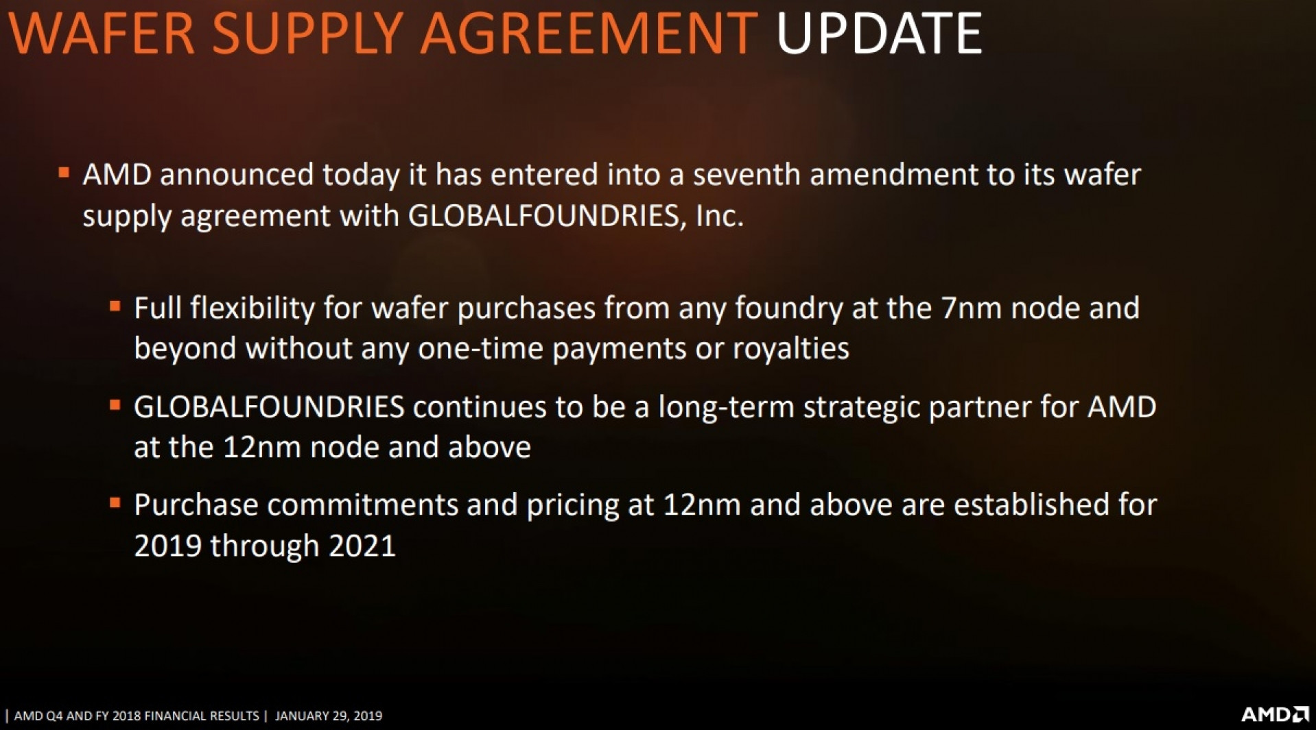
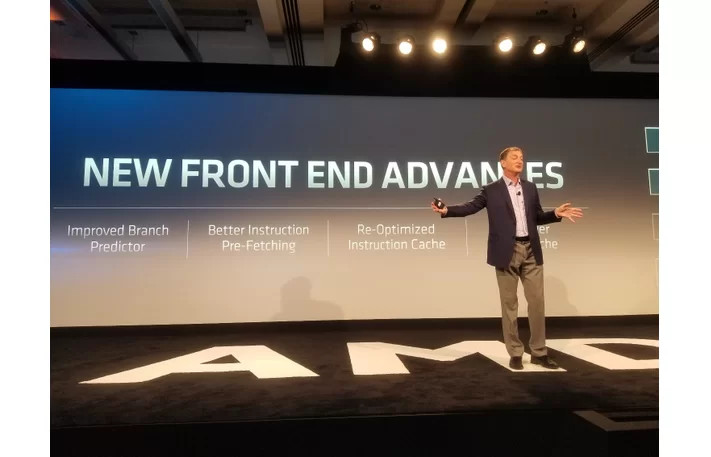
AMD Updates Wafer Supply Agreement with GlobalFoundries to Free Itself of "7nm Tax"

AMD in its Q4-2018 Earnings Report disclosed that it has amended its Wafer Supply Agreement (WSA) with GlobalFoundries that frees it from paying a "7 nanometer tax." Under the older version of WSA, AMD would have had to pay a penalty to GlobalFoundries if it sourced processors from any other semiconductor foundry. The company got preferential pricing in return for the exclusivity. With GlobalFoundries discontinuing development of cutting-edge processes such as 7 nm and 5 nm, it makes sense for AMD to seek out other foundry partners, such as TSMC, and an amendment to the WSA was needed. With this amendment in place, AMD can go ahead and source 7 nm dies from TSMC without paying penalties to GlobalFoundries (GloFo).

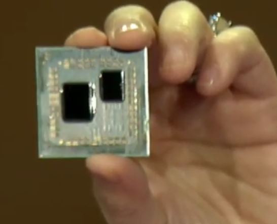
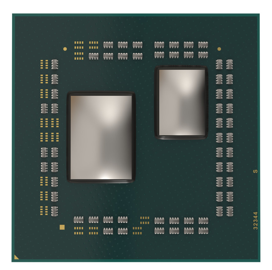
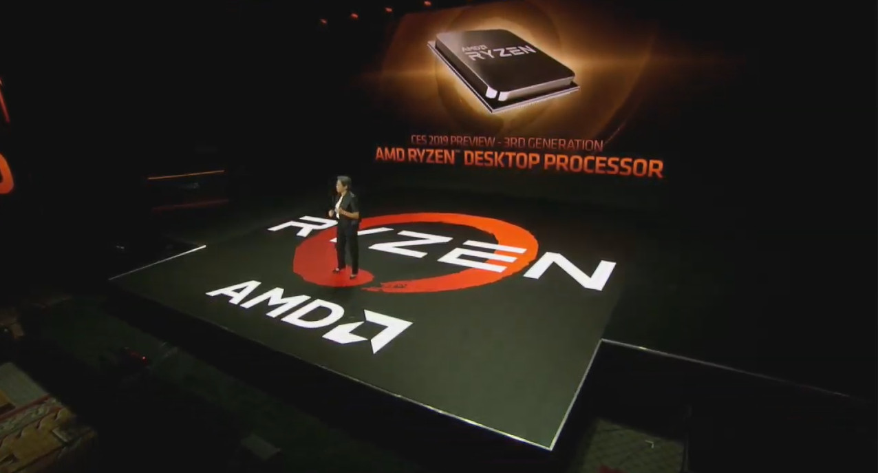
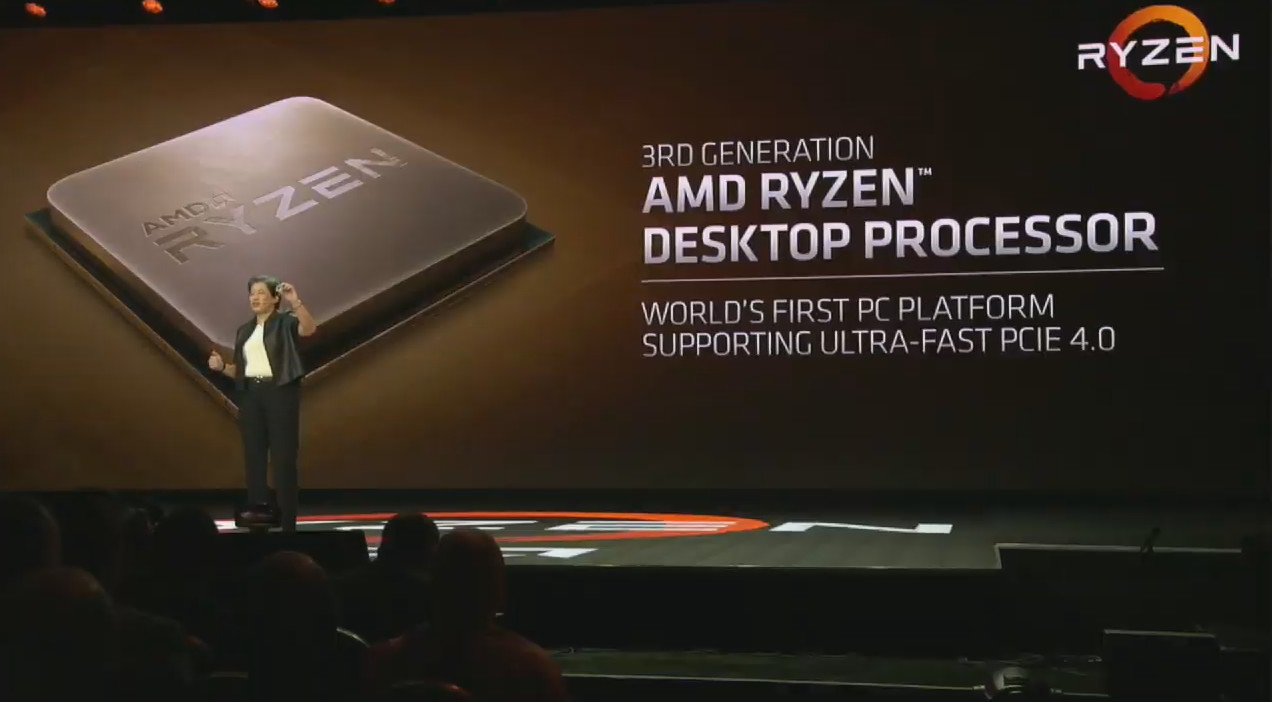
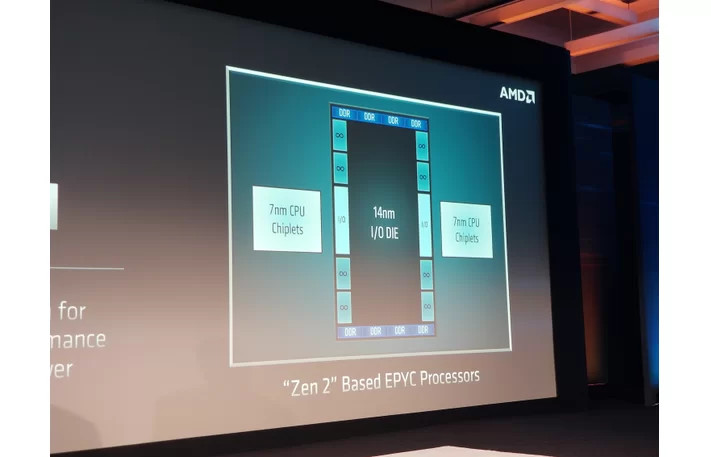
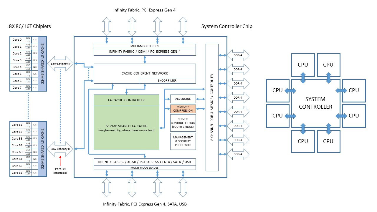
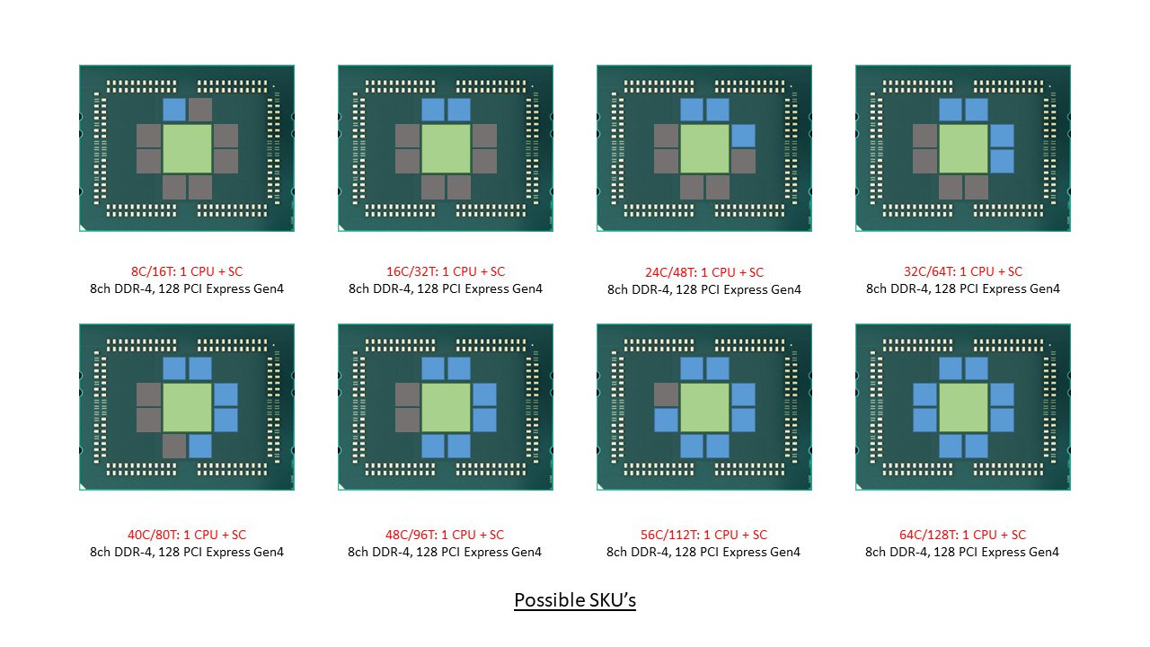
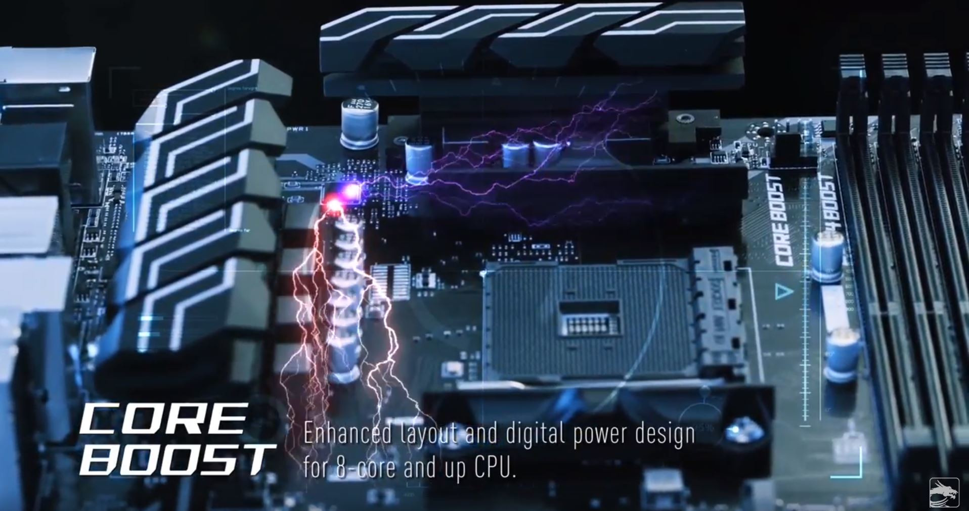
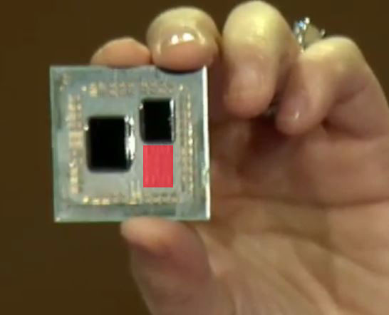
With its "Zen 2" microarchitecture, AMD is going big on multi-chip modules, in which only those components that can tangibly benefit from the switch to the 7 nm node, namely the CPU cores, would be built on 7 nm dies, called "CPU chiplets," while components that don't need the miniaturization just yet, such as the processor's memory controller, PCIe root-complex, etc., will be built on separate dies called "I/O controllers." These dies will continue to be 14 nm, and likely supplied by GloFo. Final packaging of 7 nm CPU chiplets from TSMC, and 14 nm I/O controllers from GloFo, will happen at GloFo's facilities in China or Malaysia. AMD in its amendment committed to purchasing 14 nm and 12 nm chips from GloFo between 2019 and 2021, which means the MCM approach to processors is here to stay.

ASRock Readies Nine AMD X570 Motherboards with "Zen 2" Matisse Support

Sometime mid-2019, AMD will launch its 3rd generation Ryzen "Zen 2" processors with core counts of up to 16 cores in the AM4 package. These processors will launch alongside the new AMD 500-series desktop chipset family, led by the X570. AMD assures backwards compatibility of these processors with older chipsets provided motherboard vendors support their customers with BIOS updates. You'll probably need a 500-series chipset motherboard to use PCI-Express gen 4.0 connectivity, while older chipsets will limit connectivity to gen 3.0 (not that there are any GPUs that use gen 4.0).

ASRock is developing as many as nine motherboard models based on the AMD X570, according to a list scored by VideoCardz. These include the X570 Phantom Gaming X and X570 Taichi leading the top-end; X570 Phantom Gaming 6, X570 Phantom Gaming 4, and X570 Extreme4 covering the mid-range, and the entry-level of the lineup consisting of the X570 Pro4/R2.0 and X570M Pro4/R2.0.

AMD 3rd Gen Ryzen AM4 Package Capable of Two 8-core Chiplets

At its CES 2019 keynote, AMD unveiled two killer client-segment products, the Radeon VII graphics card, which beats the GeForce RTX 2080; and a sneak preview of the 3rd generation Ryzen socket AM4 processor based on the company's "Zen 2" microarchitecture. As part of the unveil, CEO Lisa Su demonstrated an 8-core/16-thread 3rd generation Ryzen prototype processor in a head-to-head CineBench nT face-off with the Intel Core i9-9900K processor, which has the same core-count. The Ryzen narrowly beat the Intel flagship. Following this, Dr. Su held up a de-lidded sibling of the processor that was tested, revealing not one, but two dies.

This confirms that AMD is taking the heterogeneous multi-chip module approach to building its 3rd generation Ryzen processors, much like its 2nd generation EPYC processors that were unveiled late last year. The MCM of the processor Dr. Su held up had two chips, the smaller chip is an 8-core CPU chiplet built on the 7 nm process, that appears to have the same die-size as the 8-core chiplets that make up the 64-core 2nd gen EPYC MCMs, the larger die is an I/O controller logic built on the 14 nm process. This die controls the memory, PCIe, and SoC connectivity of the package. We noticed something curious about the way the two dies are arranged on the package substrate.

AMD's CES 2019 Keynote - Stream & Live Blog

CPUs or GPUs? Ryzen 3000 series up to 16 cores or keeping their eight? Support for raytracing? Navi or die-shrunk Vega for consumer graphics? The questions around AMD's plans for 2019 are still very much in the open, but AMD's Lisa Su's impending livestream should field the answers to many of these questions, so be sure to watch the full livestream, happening in just a moment.

You can find the live stream here, at YouTube.

18:33 UTC: Looking forward, Lisa mentioned a few technology names without giving additional details: "... when you're talking about future cores, Zen 2, Zen 3, Zen 4, Zen 5, Navi, we're putting all of these architectures together, in new ways".

18:20 UTC: New Ryzen 3rd generation processors have been teased. The upcoming processors are based on Zen 2, using 7 nanometer technology. AMD showed a live demo of Forza Horizon 4, using Ryzen third generation, paired with Radeon Vega VII, which is running "consistently over 100 FPS at highest details at 1080p resolution". A second demo, using Cinebench, pitted an 8-core/16-thread Ryzen 3rd generation processor against the Intel Core i9-9900K. The Ryzen CPU was "not final frequency, an early sample". Ryzen achieved a score of 2057 using 135 W, while Intel achieved a score of 2040 using 180 W.. things are looking good for Ryzen 3rd generation indeed. Lisa also confirmed that next-gen Ryzen will support PCI-Express 4.0, which doubles the bandwidth per lane over PCI-Express 3.0. Ryzen third generation will run on the same AM4 infrastructure as current Ryzen; all existing users of Ryzen can simply upgrade to the new processors, when they launch in the middle of 2019 (we think Computex).
Ryzen third generation uses a chiplet design. The smaller die on the right contains 8-cores/16-threads using 7 nanometer technology. The larger die on the left is the IO die, which consists of things like the memory controller and PCI-Express connectivity, to shuffle data between the CPU core die and the rest of the system.

AMD-hired Agency in South Korea Teases AMD Ryzen 7 3700X, Ryzen 5 3600X

Anyone looking for an update to their CPU that didn't quite jump on the Coffee Lake/Zen/Zen+ bandwagon is likely paying close attention to AMD's upcoming Zen 2 CPUs. The upcoming AMD processors will finally leave the company ahead of Intel in terms of manufacturing process for the first time in years, and will bring about AMD's new vision for HCC desktop processors in a chiplet design. With the release of Zen 2 set for 2019 (probably around Computex), and its launch being of such importance to AMD, it isn't that surprising that some promotions/teases are already popping up.

The tease in question was posted by an AMD-contracted Sales agency in South Korea, which launched a campaign inviting users to guess Cinebench scores for upcoming AMD processors: namely, the Ryzen 7 3700X and Ryzen 5 3600X - thus confirming the nomenclature for AMD's upcoming CPUs. The contest finishes on December 14th, and is basically asking users to take a gander on scores for unreleased CPUs - promising prizes of said CPUs when they launch.

AMD 3rd Generation Ryzen Probable SKUs, Specs, Pricing Leaked?

One of our readers tipped us off with a very plausible looking image that drops a motherlode of information about what AMD's 2nd generation Ryzen (aka Ryzen 3000 series) processor lineup could look like. This includes a vast selection of SKUs, their CPU and iGPU core configurations, clock-speeds, and OEM channel pricing. The list speaks of a reentry for 7th generation A-series "Excavator" as Duron X4 series, followed by Duron 300GE-series based on a highly cut down "Raven Ridge," Athlon 300GE 2-core/4-thread based on an implausible "Zen+ 12 nm" APU die, followed by quad-core Ryzen 3 3000 series processors with and without iGPUs, making up the company's entry-level product lineup.

The core counts seem to jump from 4-core straight to 8-core, with no 6-core in between, for the Ryzen 5 series. This is also where AMD's new IP, the 7 nm "Zen 2" architecture, begins. There appears to be a large APU die (or a 3-chip MCM) with an 8-core CPU and 20-CU iGPU, which makes up certain Ryzen 5 SKUs. These chips are either 8-core/8-thread or 8-core/16-thread. The Ryzen 7 series is made up of 12-core/24-thread processors that are devoid of iGPU. The new Ryzen 9 series extension caps off the lineup with 16-core/32-thread SKUs. And these are just socket AM4.

AMD 3rd Generation Ryzen Confirmed for Computex 2019

In a development that could explain why Intel is frantically stitching together 10 cores with the "Comet Lake" silicon, a slide leaked from a private event hosted by motherboard major GIGABYTE reveals that AMD's third generation Ryzen desktop platform could launch as early as Computex 2019 (June). The platform will include AMD's first client-segment processor based on its "Zen 2" microarchitecture, codenamed "Matisse," and its companion chipset, the AMD X570.

3rd generation Ryzen with X570 is expected to be the world's first mainstream desktop platform to feature PCI-Express gen 4.0. AMD could maintain the processor's backwards compatibility with older 300-series and 400-series chipset motherboards by shaping its PCI-Express implementation to use external re-drivers based on the motherboard. This could make 500-series motherboards slightly pricier than current AM4 motherboards. Backwards compatibility could mean that unless you really need PCIe gen 4.0, you should be able to save money by opting for older motherboards.

AMD Doubles L3 Cache Per CCX with Zen 2 "Rome"

A SiSoft SANDRA results database entry for a 2P AMD "Rome" EPYC machine sheds light on the lower cache hierarchy. Each 64-core EPYC "Rome" processor is made up of eight 7 nm 8-core "Zen 2" CPU chiplets, which converge at a 14 nm I/O controller die, which handles memory and PCIe connectivity of the processor. The result mentions cache hierarchy, with 512 KB dedicated L2 cache per core, and "16 x 16 MB L3." Like CPU-Z, SANDRA has the ability to see L3 cache by arrangement. For the Ryzen 7 2700X, it reads the L3 cache as "2 x 8 MB L3," corresponding to the per-CCX L3 cache amount of 8 MB.

For each 64-core "Rome" processor, there are a total of 8 chiplets. With SANDRA detecting "16 x 16 MB L3" for 64-core "Rome," it becomes highly likely that each of the 8-core chiplets features two 16 MB L3 cache slices, and that its 8 cores are split into two quad-core CCX units with 16 MB L3 cache, each. This doubling in L3 cache per CCX could help the processors cushion data transfers between the chiplet and the I/O die better. This becomes particularly important since the I/O die controls memory with its monolithic 8-channel DDR4 memory controller.

AMD Ryzen 7 3700U Shows Up With Lots of Maybes, Could Feature Zen 2

AMD's low-power Ryzen 3700U APU has been leaked. Codenamed ZM370SC4T4MFG_38/22_Y, this latest AMD processor features 4 cores and 8 threads with a base clock of 2.2 GHz and a boost clock of 3.8 GHz, making it very similar to the current generation 2700U. The GPU, which is recognized as Picasso by UserBenchmark, is like just another codename for now, as other applications are listing it as a Radeon RX Vega 10 GPU. Considering the 3000U Series is supposed to be similar to the 2000U offerings it could very well feature the same Vega 10 GPU and still be based on the Zen+ or the Zen 2 architectures. That said, nothing is confirmed, but some slides leaked from Informatica Cero suggest that the Ryzen 7 3700U could indeed feature the Zen 2 architecture. That would be fairly interesting given that the Ryzen family for laptops/convertibles have been a step behind the desktop solutions for a quite some time.

Picasso which we've been hearing about since the codename first appeared in September of 2017, looks to be nothing more than Raven Ridge manufactured on the 12nm node. This is of course based on the information that is available. Some people suggest this new APU could be on the 7 nm node, but this is difficult to believe as AMD is likely to devote 7 nm manufacturing to their EPYC server solutions and Ryzen desktop products first. Therefore Zen 2 APUs for notebooks are likely still far off.

Stuttgart-based HLRS to Build a Supercomputer with 10,000 64-core Zen 2 Processors

Höchstleistungsrechenzentrum (HLRS, or High-Performance Computing Center), based in Stuttgart Germany, is building a new cluster supercomputer powered by 10,000 AMD Zen 2 "Rome" 64-core processors, making up 640,000 cores. Called "Hawk," the supercomputer will be HLRS' flagship product, and will open its doors to business in 2019. The slide-deck for Hawk makes a fascinating disclosure about the processors it's based on.

Apparently, each of the 64-core "Rome" EPYC processors has a guaranteed clock-speed of 2.35 GHz. This would mean at maximum load (with all cores loaded 100%), the processor can manage to run at 2.35 GHz. This is important, because the supercomputer's advertised throughput is calculated on this basis, and clients draw up SLAs on throughput. The advertised peak throughput for the whole system is 24.06 petaFLOP/s, although the company is yet to put out nominal/guaranteed performance numbers (which it will only after first-hand testing). The system features 665 TB of RAM, and 26,000 TB of storage.

AMD "Zen 2" IPC 29 Percent Higher than "Zen"

AMD reportedly put out its IPC (instructions per clock) performance guidance for its upcoming "Zen 2" micro-architecture in a version of its Next Horizon investor meeting, and the numbers are staggering. The next-generation CPU architecture provides a massive 29 percent IPC uplift over the original "Zen" architecture. While not developed for the enterprise segment, the stopgap "Zen+" architecture brought about 3-5 percent IPC uplifts over "Zen" on the backs of faster on-die caches and improved Precision Boost algorithms. "Zen 2" is being developed for the 7 nm silicon fabrication process, and on the "Rome" MCM, is part of the 8-core chiplets that aren't subdivided into CCX (8 cores per CCX).

According to Expreview, AMD conducted DKERN + RSA test for integer and floating point units, to arrive at a performance index of 4.53, compared to 3.5 of first-generation Zen, which is a 29.4 percent IPC uplift (loosely interchangeable with single-core performance). "Zen 2" goes a step beyond "Zen+," with its designers turning their attention to critical components that contribute significantly toward IPC - the core's front-end, and the number-crunching machinery, FPU. The front-end of "Zen" and "Zen+" cores are believed to be refinements of previous-generation architectures such as "Excavator." Zen 2 gets a brand-new front-end that's better optimized to distribute and collect workloads between the various on-die components of the core. The number-crunching machinery gets bolstered by 256-bit FPUs, and generally wider execution pipelines and windows. These come together yielding the IPC uplift. "Zen 2" will get its first commercial outing with AMD's 2nd generation EPYC "Rome" 64-core enterprise processors.

Update Nov 14: AMD has issued the following statement regarding these claims.
As we demonstrated at our Next Horizon event last week, our next-generation AMD EPYC server processor based on the new 'Zen 2' core delivers significant performance improvements as a result of both architectural advances and 7nm process technology. Some news media interpreted a 'Zen 2' comment in the press release footnotes to be a specific IPC uplift claim. The data in the footnote represented the performance improvement in a microbenchmark for a specific financial services workload which benefits from both integer and floating point performance improvements and is not intended to quantify the IPC increase a user should expect to see across a wide range of applications. We will provide additional details on 'Zen 2' IPC improvements, and more importantly how the combination of our next-generation architecture and advanced 7nm process technology deliver more performance per socket, when the products launch.

AMD Zen 2 "Rome" MCM Pictured Up Close

Here is the clearest picture of AMD "Rome," codename for the company's next-generation EPYC socket SP3r2 processor, which is a multi-chip module of 9 chiplets (up from four). While first-generation EPYC MCMs (and Ryzen Threadripper) were essentially "4P-on-a-stick," the new "Rome" MCM takes the concept further, by introducing a new centralized uncore component called the I/O die. Up to eight 7 nm "Zen 2" CPU dies surround this large 14 nm die, and connect to it via substrate, using InfinityFabric, without needing a silicon interposer. Each CPU chiplet features 8 cores, and hence we have 64 cores in total.

The CPU dies themselves are significantly smaller than current-generation "Zeppelin" dies, although looking at their size, we're not sure if they're packing disabled integrated memory controllers or PCIe roots anymore. While the transition to 7 nm can be expected to significantly reduce die size, groups of two dies appear to be making up the die-area of a single "Zeppelin." It's possible that the CPU chiplets in "Rome" physically lack an integrated northbridge and southbridge, and only feature a broad InfinityFabric interface. The I/O die handles memory, PCIe, and southbridge functions, featuring an 8-channel DDR4 memory interface that's as monolithic as Intel's implementations, a PCI-Express gen 4.0 root-complex, and other I/O.

AMD Unveils "Zen 2" CPU Architecture and 7 nm Vega Radeon Instinct MI60 at New Horizon

AMD today held its "New Horizon" event for investors, offering guidance and "color" on what the company's near-future could look like. At the event, the company formally launched its Radeon Instinct MI60 GPU-based compute accelerator; and disclosed a few interesting tidbits on its next-generation "Zen 2" mircroarchitecture. The Instinct MI60 is the world's first GPU built on the 7 nanometer silicon fabrication process, and among the first commercially available products built on 7 nm. "Rome" is on track to becoming the first 7 nm processor, and is based on the Zen 2 architecture.

The Radeon Instinct MI60 is based on a 7 nm rendition of the "Vega" architecture. It is not an optical shrink of "Vega 10," and could have more number-crunching machinery, and an HBM2 memory interface that's twice as wide that can hold double the memory. It also features on-die logic that gives it hardware virtualization, which could be a boon for cloud-computing providers.

AMD's Zen 2 Could be Revealed on November 6th, "Next Horizon" Event Scheduled

AMD Investor Relations will host a "Next Horizon" event on November 6th, and although there is no confirmation on what products will be announced there, the title alone makes us think about AMD's Zen 2 architecture. The company has just explained that on that day their executives will "discuss the innovation of AMD products and technology, specifically designed with the datacenter on industry-leading 7 nm process technology". AMD announced Ryzen and quite a lot of details about the Zen's processors on their last "Horizon" event, so it seems plausible that the incoming event will be perfect to talk about its next-gen architecture. That focus on the 7 nm process technology will probably make AMD talk about their new Vega graphics, but it seems end users will have to wait, as datacenters come first.

AMD Could Solve Memory Bottlenecks of its MCM CPUs by Disintegrating the Northbridge

AMD sprung back to competitiveness in the datacenter market with its EPYC enterprise processors, which are multi-chip modules of up to four 8-core dies. Each die has its own integrated northbridge, which controls 2-channel DDR4 memory, and a 32-lane PCI-Express gen 3.0 root complex. In applications that can not only utilize more cores, but also that are memory bandwidth intensive, this approach to non-localized memory presents design bottlenecks. The Ryzen Threadripper WX family highlights many of these bottlenecks, where video encoding benchmarks that are memory-intensive see performance drops as dies without direct access to I/O are starved of memory bandwidth. AMD's solution to this problem is by designing CPU dies with a disabled northbridge (the part of the die with memory controllers and PCIe root complex). This solution could be implemented in its upcoming 2nd generation EPYC processors, codenamed "Rome."

With its "Zen 2" generation, AMD could develop CPU dies in which the integrated northrbidge can be completely disabled (just like the "compute dies" on Threadripper WX processors, which don't have direct memory/PCIe access relying entirely on InfinityFabric). These dies talk to an external die called "System Controller" over a broader InfinityFabric interface. AMD's next-generation MCMs could see a centralized System Controller die that's surrounded by CPU dies, which could all be sitting on a silicon interposer, the same kind found on "Vega 10" and "Fiji" GPUs. An interposer is a silicon die that facilitates high-density microscopic wiring between dies in an MCM. These explosive speculative details and more were put out by Singapore-based @chiakokhua, aka The Retired Engineer, a retired VLSI engineer, who drew block diagrams himself.

AMD Zen 2 GNU Compiler Patch Published, Exposes New Instruction Sets

With a November deadline for feature freeze fast approaching, GNU toolchain developers are now adding the last feature additions to GCC 9.0 (GNU Compiler Collection). Ahead of that deadline, AMD has released their first basic patch adding the "znver2" target and therefore Zen 2 support to GCC. While the patch uses the same cost tables and scheduler data as Znver1, it does feature three new instructions that will be available to AMD's next-gen CPUs which include; Cache Line Write Back (CLWB), Read Processor ID (RDPID), and Write Back and Do Not Invalidate Cache (WBNOINVD).

These three instructions are the only ones that have been found thus far by digging through the current code. Taking into account this is the first patch it can be considered a jumping off point, making sure that the GCC 9.1 stable update, which comes out in 2019, has support for Zen 2. Further optimizations and instructions may be implemented in the future. This is likely since AMD has yet to update the scheduler cost tables and by extension means they may not want to reveal everything about Zen 2 just yet. You could say AMD is for now playing it safe, at least until their 7nm EPYC 2 processors launch in 2019.

AMD "Vega 20" GPU Not Before Late Q1-2019

AMD "Vega 20" is a new GPU based on existing "Vega" graphics architecture, which will be fabbed on the 7 nanometer silicon fabrication process, and bolstered with up to 32 GB of HBM2 memory across a 4096-bit memory interface that's double the bus-width of "Vega 10". AMD CEO Lisa Su already exhibited a mock-up of this chip at Computex 2018, with an word that alongside its "Zen 2" based EPYC enterprise processors, "Vega 20" will be the first 7 nm GPU. AMD could still make good on that word, only don't expect to find one under your tree this Holiday.

According to GamersNexus, the first "Vega 20" products won't launch before the turn of the year, and even in 2019, one can expect product launches till the end of Q1 (before April). GamersNexus cites reliable sources hinting at the later-than-expected arrival of "Vega 20" as part of refuting alleged "Final Fantasy XV" benchmarks of purported "Vega 20" engineering samples doing rounds on the web. Lisa Su stressed the importance of data-center GPUs in AMD's Q3-2018 earnings call, which could hint at the possibility of AMD allocating its first "Vega 20" yields to high-margin enterprise brands such as Radeon Pro and Radeon Instinct.

AMD Zen 2 Offers a 13% IPC Gain over Zen+, 16% over Zen 1

AMD "Zen" CPU architecture brought the company back to competitive relevance in the processor market. It got an incremental update in the form of "Zen+" which saw the implementation of an improved 12 nm process, and improved multi-core boosting algorithm, along with improvements to the cache subsystem. AMD is banking on Zen 2 to not only add IPC (instructions per clock) improvements; but also a new round of core-count increases. Bits n Chips has information that Zen 2 is making significant IPC gains.

According to the Italian tech publication, we could expect Zen 2 IPC gains of 13 percent over Zen+, which in turn posted 2-5% IPC gains over the original Zen. Bits n Chips notes that these IPC gains were tested in scientific tasks, and not in gaming. There is no gaming performance data at the moment. AMD is expected to debut Zen 2 with its 2nd generation EPYC enterprise processors by the end of the year, built on the 7 nm silicon fabrication process. This roughly 16 percent IPC gain versus the original Zen, coupled with higher clocks, and possibly more cores, could complete the value proposition of 2nd gen EPYC. Zen 2-based client-segment products can be expected only in 2019.

AMD Fast-tracks 7nm "Navi" GPU to Late-2018 Alongside "Zen 2" CPU

AMD is unique in the world of computing as the only company with both high-performance CPU and GPU products. For the past several years we have been executing our multi-generational leadership product and architectural roadmap. Just in the last 18 months, we successfully introduced and ramped our strongest set of products in more than a decade and our business has grown dramatically as we gained market share across the PC, gaming and datacenter markets.

The industry is at a significant inflection point as the pace of Moore's Law slows while the demand for computing and graphics performance continues to grow. This trend is fueling significant shifts throughout the industry and creating new opportunities for companies that can successfully bring together architectural, packaging, system and software innovations with leading-edge process technologies. That is why at AMD we have invested heavily in our architecture and product roadmaps, while also making the strategic decision to bet big on the 7nm process node. While it is still too early to provide more details on the architectural and product advances we have in store with our next wave of products, it is the right time to provide more detail on the flexible foundry sourcing strategy we put in place several years ago.

Rumor: AMD's Zen 2, 7 nm Chips to Feature 10-15% IPC Uplift, Revised 8-core per CCX Design

A post via Chiphell makes some substantial claims on AMD's upcoming Zen 2 microarchitecture, built on the 7 nm process. AMD has definitely won the core-count war once again (albeit with a much more decisive blow to Intel's dominance than with Bulldozer), but the IPC battle has been an uphill one against Intel's slow, but sure, improvement in that area over the years. AMD did say, at the time they introduced the Zen architecture, that they had a solid understanding on Zen's choke points and its improveable bits and pieces - and took it to heart to deliver just that.

MSI Drops First Hint of AMD Increasing AM4 CPU Core Counts

With Intel frantically working on an 8-core socket LGA1151 processor to convincingly beat the 8-core AMD Ryzen 2000 series processor, AMD could be working on the next cycle of core-count increases for the mainstream-desktop platform. Motherboard maker MSI may have dropped the first hint that AMD is bringing >8 cores to the socket AM4 mainstream-desktop platform by mentioning that its upcoming motherboards based on the AMD B450 chipset support 8-core "and up" CPU in a marketing video.

AMD will get its next opportunity to tinker with key aspects of its CPU micro-architecture with "Zen 2," being built on the 7 nm silicon fabrication process. If it decides to stick with the CCX approach to multi-core processors, the company could increase per-CCX core counts. A 50 percent core-count increase enables 12-core processors, while a 100 percent increase brings 16-cores to the AM4 platform. MSI video confirms that these >8-core processors will have backwards-compatibility with existing 400-series chipsets, even if they launch alongside newer 500-series chipset.
The video follows.

AMD Vega 20 GPU Could Implement PCI-Express gen 4.0

The "Vega 20" silicon will be significantly different from the "Vega 10" which powers the company's current Radeon RX Vega series. AMD CEO Dr. Lisa Su unveiled the "Vega 20" silicon at the company's 2018 Computex event, revealing that the multi-chip module's 7 nm GPU die is surrounded by not two, but four HBM2 memory stacks, making up to 32 GB of memory. Another key specification is emerging thanks to the sharp eyes at ComputerBase.de - system bus.

A close inspection of the latest AMDGPU Linux driver includes PCI-Express link speed definitions for PCI-Express gen 4.0, which offers 256 Gbps of bandwidth per direction at x16 bus width, double that of PCI-Express gen 3.0. "Vega 20" got its first PCIe gen 4.0 support confirmation from a leak slide that surfaced around CES 2018. AMD "Vega" architecture slides from last year hinted at a Q3/Q4 launch of the first "Vega 20" based product. The same slide also hinted that the next-generation EPYC processor, which we know are "Zen 2" based and not "Zen+," could feature PCI-Express gen 4.0 root-complexes. Since EPYC chips are multi-chip modules, it could also hint at the likelihood of PCIe gen 4.0 on "Zen 2" based 3rd generation Ryzen processor family.

AMD to Begin Sampling 7nm "Zen 2" Processors Within 2018 for a 2019 Launch

It looks like AMD's processor product launch cycle is on steroids, and keeping up (or even ahead) of Intel. After launching the first 12 nm processor architecture with "Zen+," the company is giving final touches to what it hopes to be the world's first 7 nanometer processor architecture, with "Zen 2." The company will reportedly begin sampling the chip within 2018, to enable volume production and market launch in 2019. Speaking at an investors conference call following the company's Q1-2018 Results release, AMD CEO Dr. Lisa Su confirmed the 7 nm roll-out strategy of her company.

"We have a 7nm GPU based on Vega that we'll sample later this year. We have a 7nm server CPU that we'll sample later this year. And then, obviously, we have a number of products that are planned for 2019 as well. So it's a very, very busy product season for us. But we're pleased with the sort of the execution on the product roadmap," Dr. Su said. Unlike Zen+, Zen 2 is a major update to the company's processor micro-architecture, and presents the company with opportunities to improve several silicon-level specifications, such as the number of cores per CCX, the IPC of each core, the core-count of the die, the cache hierarchy, and the overall energy-efficiency.

AMD Works on "Zen 5" Micro-architecture Already

AMD late Monday posted a video of key people associated with the company's successful Ryzen processor family, to walk down memory lane and stare into the future, on its official YouTube channel. Mike Clark, who holds the designation of Sr. Fellow Design Engineering at AMD, stated that he is "already working on Zen 5." Going by AMD's naming convention, the number next to "Zen" denotes major micro-architecture generation since "Zen" and any "+" following the number denotes refinement to a newer silicon fabrication node. "Zen+," for example, is a refinement of "Zen 1" or simply "Zen" to the newer 12 nm process, and allows AMD engineers to make minor improvements without any major design changes.

On the other hand, "Zen 2" presents AMD with the opportunity to bring about major design changes (think "more than 4 cores per CCX"), or even improvements within the core itself. "Zen 5" is hence the fifth major micro-architecture chance since "Zen," although it would be premature to call it "6th generation Ryzen," as there could be several "+" stopgaps between "Zen +" and "Zen 5." To ensure people don't dismiss Clark's words for a slip of the tongue, AMD even annotated "Yes, he said Zen 5, see Endnote," and in the Endnote that has a lot of CYA statements, confirmed that "Zen 5" is a legit internal code-name for a micro-architecture AMD is working on.
The video follows.

AMD Readies Ryzen Threadripper SKUs based on "Pinnacle Ridge" Dies

Hot on the heels of this morning's big AMD Ryzen 2000-series slide dump, comes a new roadmap slide that gives a larger overview of how AMD is addressing various client processor market segments. It begins with the mention of a 2nd generation Ryzen Threadripper series launch within 2018. These chips presumably, are multi-chip modules of the company's new 12 nm "Pinnacle Ridge" silicon, and will be compatible with existing AMD X399 chipset motherboards through BIOS updates. The "Pinnacle Ridge" silicon supports higher clock-speeds, has several microarchitecture refinements, and a few new overclocker-centric features.

The better news is that company seems to be updating its HEDT processor lineup every year; and that the current Threadripper series isn't a one-off halo product like its Athlon64 FX "QuadFX" 2P platform. With "Pinnacle Ridge" based Threadripper 2000-series MCMs slated for 2018; 2019 will see the launch of the new "Castle Peak" HEDT processor. It's not known if this is an MCM. The spiritual successor to "Pinnacle Ridge" is "Matisse." This is Zen 2 based, and will have significant changes to the core design, presenting AMD with an opportunity to review the way it arranges cores. "Picasso" succeeds "Raven Ridge" as the company's Zen 2-based APUs. "Picasso," along with "Matisse" and "Castle Peak" could see AMD implement GlobalFoundries' new 7 nm silicon fabrication process, given its 2019 timeline. 2020 will see their refined avatars - an unnamed "Next-Gen HEDT" chip, "Vermeer," and "Renoir," respectively.
Return to Keyword Browsing
May 21st, 2024 07:34 EDT change timezone

New Forum Posts

Popular Reviews

Controversial News Posts