News Posts matching #Zen 2

Return to Keyword Browsing

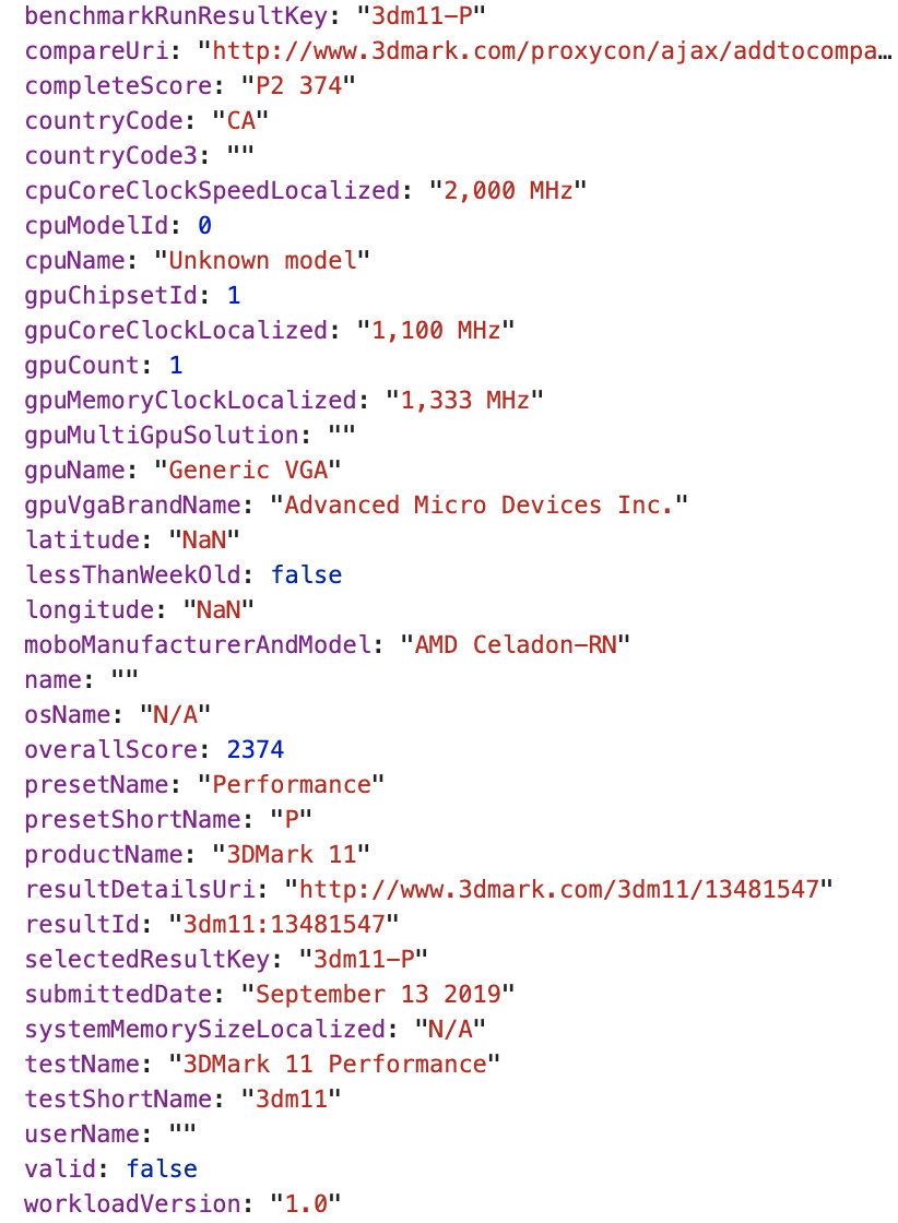
Sony's Mark Cerny to Detail PS5 Architecture March 18th

Sony has announced via Twitter that their lead system architect Mark Cerny will "provide a deep dive into PS5's system architecture, and how it will shape the future of games" tomorrow. This is likely the start of Sony's marketing campaign for the release of the PS5 which is due out Holidays 2020.

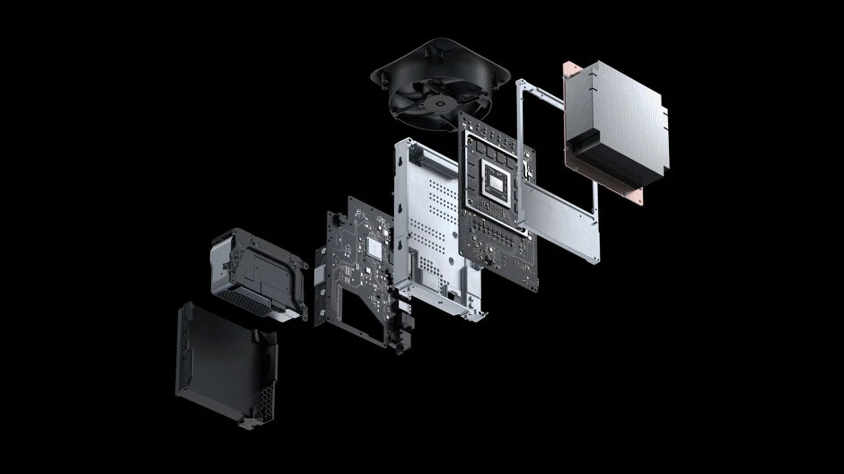
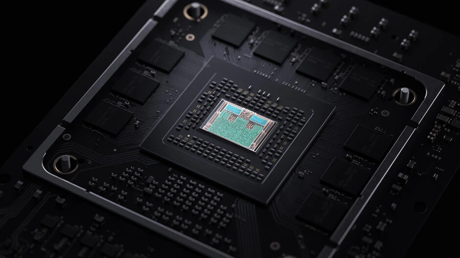
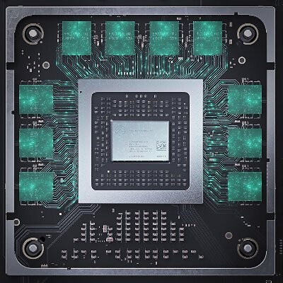
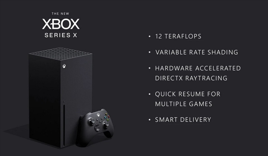
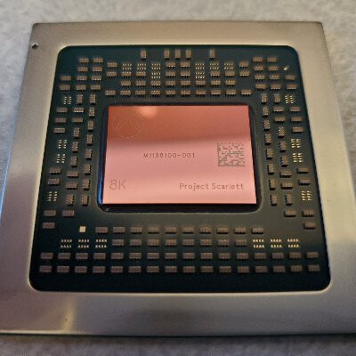
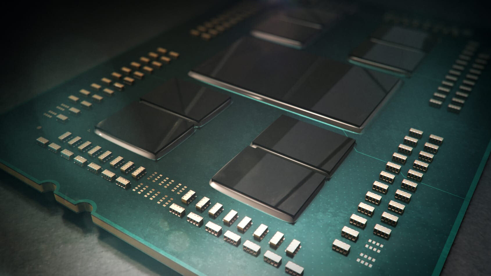
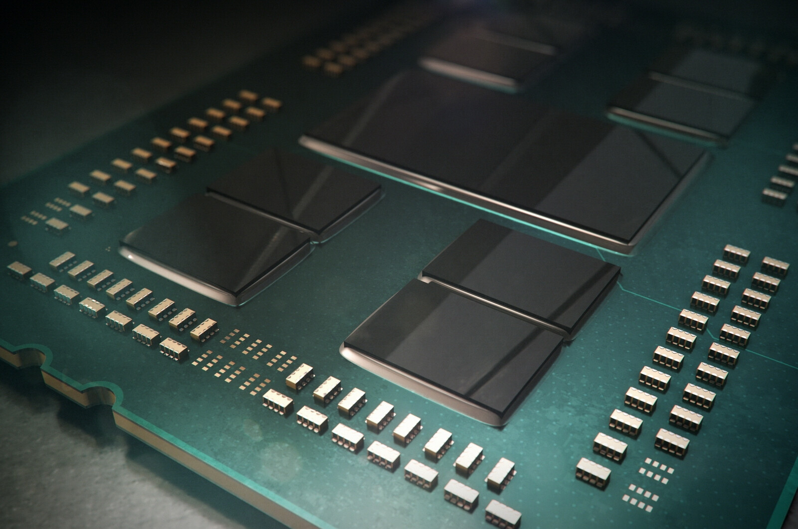
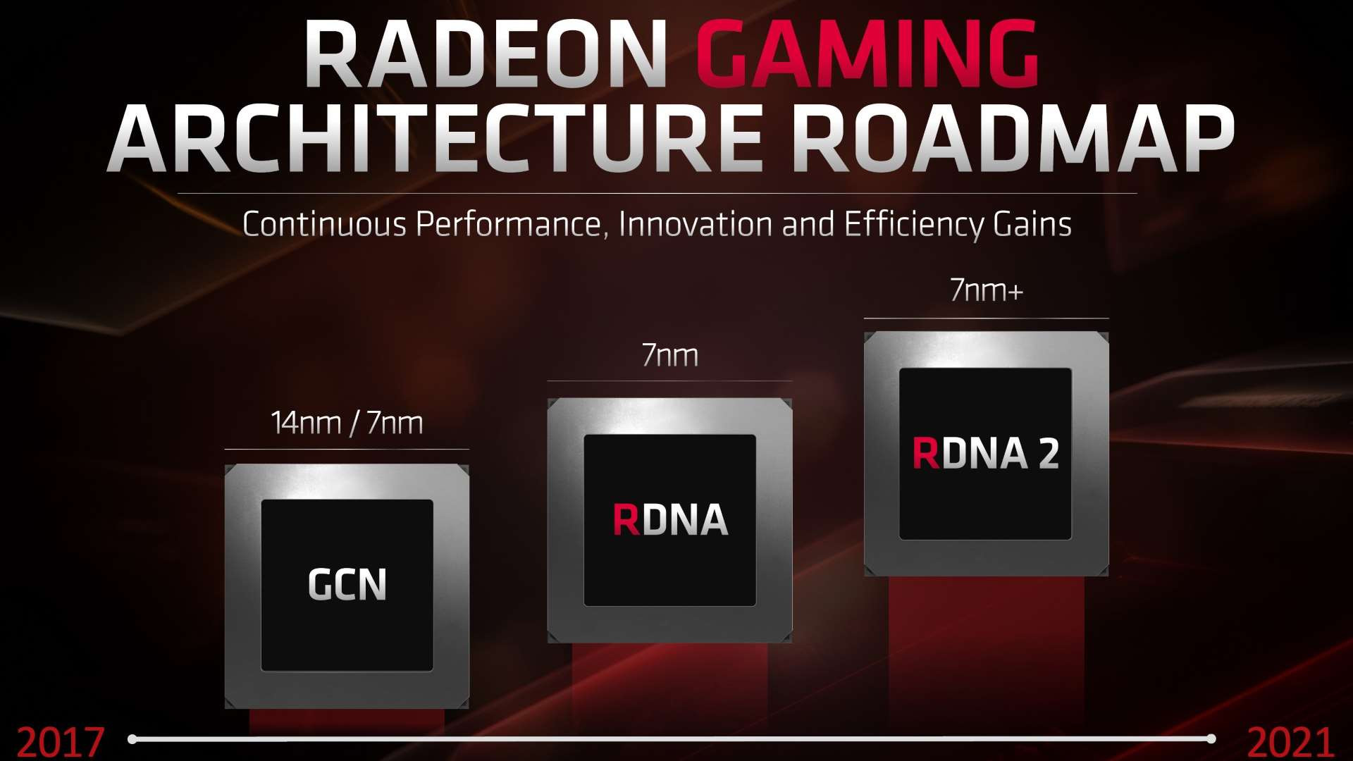
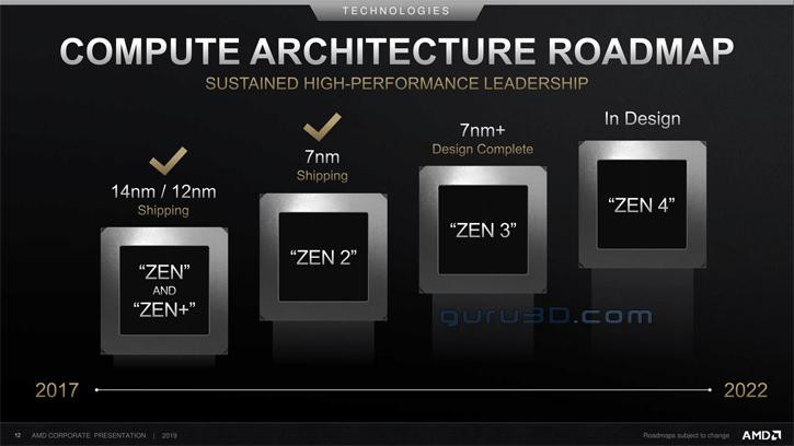
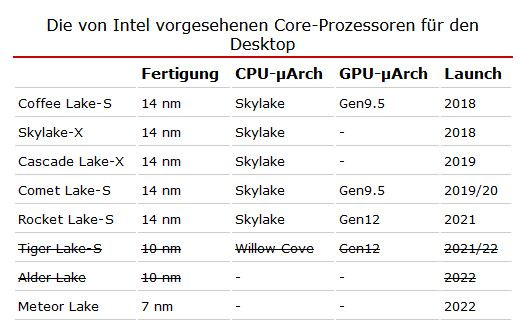
The Japanese company has remained puzzlingly tight-lipped regarding their next-gen games console, which is a far cry from Microsoft's position, who have been releasing details and teasing their next-gen Xbox Series X system for a while now. It remains to be seen how Sony's system will differ from Microsoft's Xbox Series X, since most specs are rumored to be close on both consoles. The underlying Zen 2 architecture for the CPUs is confirmed in both consoles, and so should the fabrication process and RDNA2-based graphics with dedicated ray tracing hardware. It remains to be seen how the companies will aim to differentiate their offerings.

Complete Hardware Specs Sheet of Xbox Series X Revealed

Microsoft just put out of the complete hardware specs-sheet of its next-generation Xbox Series X entertainment system. The list of hardware can go toe to toe with any modern gaming desktop, and even at its production scale, we're not sure if Microsoft can break-even at around $500, possibly counting on game and DLC sales to recover some of the costs and turn a profit. To begin with the semi-custom SoC at the heart of the beast, Microsoft partnered with AMD to deploy its current-generation "Zen 2" x86-64 CPU cores. Microsoft confirmed that the SoC will be built on the 7 nm "enhanced" process (very likely TSMC N7P). Its die-size is 360.45 mm².

The chip packs 8 "Zen 2" cores, with SMT enabling 16 logical processors, a humongous step up from the 8-core "Jaguar enhanced" CPU driving the Xbox One X. CPU clock speeds are somewhat vague. It points to 3.80 GHz nominal and 3.66 GHz with SMT enabled. Perhaps the console can toggle SMT somehow (possibly depending on whether a game requests it). There's no word on the CPU's cache sizes.

Xbox Series X Semi-custom SoC Features 320-bit Memory Interface, 10 GB or 20 GB Memory

Microsoft's upcoming Xbox Series X entertainment system is shaping up to be a technological monstrosity. Xbox group head at Microsoft, Phil Spencer, last revealed a picture of its semi-custom SoC back in January, by setting it as his Twitter display picture. Over the following weeks, many more technical details, such as the chip's 12 TFLOP/s combined compute power, would be let out. Spencer updated his display picture revealing a segment of the Xbox Series X mainboard with the SoC and memory chips surrounding it. The picture reveals the large SoC package in the center, surrounded on three sides by ten memory chips, possibly GDDR6, each with its own wiring to the SoC. This indicates that the SoC features a 320-bit wide memory interface.

As for the memory density, there's no way to tell. It could be 10 GB if those are 8 Gbit memory chips, or 20 GB if those are 16 Gbit. It boils down to which device the Xbox Series X the company wants to succeed. The Xbox One S features 8 GB of DDR3, while the spruced up Xbox One X features 12 GB of GDDR5. If the new Xbox Series X succeeds the latter, then it could very well feature 20 GB, more so given Microsoft's lofty design goals (4K UHD gaming with real-time ray-tracing). Microsoft leverages hUMA to use a common memory pool for both the CPU and GPU. Designed in collaboration with AMD on a TSMC 7 nm-class node (likely the N7P), the SoC features "Zen 2" CPU cores, and a GPU based on the RDNA2 graphics architecture.
Xbox Series X memory

AMD Processors Since 2011 Hit with Cache Attack Vulnerabilities: Take A Way

Cybersecurity researcher Moritz Lipp and his colleagues from the Graz University of Technology and the University of Rennes uncovered two new security vulnerabilities affecting all AMD CPU microarchitectures going back to 2011, detailed in a research paper titled "Take A Way." These include "Bulldozer" and its derivatives ("Piledriver," "Excavator," etc.,) and the newer "Zen," "Zen+," and "Zen 2" microarchitectures. The vulnerabilities are specific to AMD's proprietary L1D cache way predictor component. It is described in the security paper's abstract as a means for the processor to "predict in which cache way a certain address is located, so that consequently only that way is accessed, reducing the processor's power consumption."

By reverse engineering the L1D cache way predictor in AMD microarchitectures dating from 2011 to 2019, Lipp, et al, discovered two new attack vectors with which an attacker can monitor the victim's memory accesses. These vectors are named "Collide+Probe," and "Load+Reload." The paper describes the first vector as follows: "With Collide+Probe, an attacker can monitor a victim's memory accesses without knowledge of physical addresses or shared memory when time-sharing a logical core." The second vector is described as "With Load+Reload, we exploit the way predictor to obtain highly-accurate memory-access traces of victims on the same physical core." The two vulnerabilities have not been assigned CVE entries at the time of this writing. The research paper, however, describes the L1D cache way predictor in AMD processors as being vulnerable to attacks that can reveal contents of memory or even keys to a vulnerable AES implementation. For now there is no mitigation to these attacks, but the company is reportedly working on firmware and driver updates. Access the research paper here.
AMD L1D cache way predictor logic found vulnerable in Take A Way attack classes.

Microsoft Confirms Xbox Series X Specs - 12 TFLOPs, Custom APU With Zen 2, RDNA 2, H/W Accelerated Raytracing

Microsoft has confirmed the official specs for the Xbox Series X games console, due Holiday 2020 (think November). The new specs announcement confirms the powerhouse of a console this will be, with its peak 12 TFLOPs compute being 8 times that of the original Xbox One, and twice that of the Xbox One X, which already quite capable of powering true 4K experiences. This 12 TFLOPs figure is a mighty impressive one - just consider that AMD's current highest-performance graphics card, Radeon VII, features a peak 13.4 TFLOPs of computing power - and that's a graphics card that was launched just a year ago.

The confirmation also mentions support for Hardware-Accelerated raytracing, something that all but confirms the feature being built into AMD's RDNA 2 microarchitecture (of which we are expecting news anytime now). this, alongside Variable Rate Shading (VRS) support, brings AMD to feature parity with NVIDIA's Turing, and should allow developers to optimize their performance and graphical targets without any discernible quality loss.

Apple Finally Buying AMD CPUs? Pointers to Ryzens Found in MacOS Beta

Since its switch to the x86 machine architecture from PowerPC in the mid-2000s, Apple has been consistent with Intel as its sole supplier of CPUs for its Macbooks, iMac desktops, and Mac Pro workstations. The company's relationship with rival AMD has been limited to sourcing discrete GPUs. If pieces of code from a MacOS beta is anything to go buy, Apple could bite the AMD bullet very soon. References to several AMD processors were found in MacOS 10.15.4 Beta 1. These include the company's "Picasso," "Renoir," and "Van Gogh" APUs.

It's very likely that with increasing CPU IPC and energy-efficiency, Apple is finally seeing the value in single-chip solutions from AMD that have a good enough combination of CPU and iGPUs. The 7 nm "Renoir" silicon in particular could change the mobile and desktop computing segments, thanks to its 8-core "Zen 2" CPU, and a "Vega" based iGPU that's highly capable in non-gaming and light-gaming tasks. AMD's proprietary SmartShift feature could also be leveraged, which dynamically switches between the iGPU and an AMD discrete GPU.

AMD "Renoir" Ryzen 7 4700U Geekbenched

An unknown Lenovo notebook powered by the 15-Watt Ryzen 7 4700U "Renoir" 8-core processor was put through Geekbench. The chip yielded scores of 4910 single-core, and 21693 multi-core. This puts the 4700U ahead of the Core i7-1065G7, which is known to score around 4400 points on average in the single-core test, and around 17000 on average, in the multi-core test, falling behind due to fewer CPU cores. The 4700U features an 8-core CPU based on the "Zen 2" microarchitecture. Its desktop compatriot, the Ryzen 7 3700X, is significantly faster, with around 20% higher single-core, and over 60% higher multi-core performance. This is probably because the 3700X is unconstrained with its 65-Watt TDP and significantly higher power limits. It also has four times more L3 cache, but that's probably to cushion the IFOP interconnect between the CPU chiplet and I/O die.

AMD Rolls Out Athlon 3000 Gold and Silver "Zen" 15W Mobile SoCs

The "Zen 2" based Ryzen 4000-series mobile processors and Threadripper 3990X HEDT chip dominated headlines throughout AMD's CES 2020 event, but an important product announcement slipped past us: the mobile Athlon 3000 Gold and 3000 Silver families of entry-level mobile SoCs. These are 15-Watt SoCs targeting low-cost ultraportables, convertibles, and straight up Windows x64 tablets, competing against Intel's Pentium Gold 5000U "Whiskey Lake" and Pentium Silver "Gemini Lake Refresh" series. The family currently only consists of two SKUs, the Athlon Gold 3150U and Athlon Silver 3050U.

The two chips are based on the "Dali" silicon, and feature "Zen" CPU cores. The Athlon Gold 3150U features a 2-core/4-thread "Zen" CPU clocked at 2.40 GHz with 3.30 GHz boost. The Athlon Silver 3050U, on the other hand, is configured with a 2-core/2-thread CPU clocked at 2.30 GHz with 3.20 GHz boost. The CPUs on both models is configured with 4 MB of L3 cache, which takes their "total cache" (L2 + L3) figure up to 5 MB. The iGPU on the 3150U is a Radeon Vega 3 with 192 stream processors, clocked at 1.00 GHz. The one on the 3050U, is AMD's smallest, with just 2 compute units, working up to 128 stream processors, but the engine clock is set at 1.10 GHz.

AMD Ryzen Threadripper 3990X Pricing and Availability Detailed

AMD will update its 3rd generation Ryzen Threadripper product stack sooner than expected. The flagship 64-core/128-thread Ryzen Threadripper 3990X will be available to purchase on February 7, 2020, priced at USD $3,990. The company debuted the "Zen 2" based 3rd gen Threadripper family last November with the 24-core Threadripper 3960X and the 32-core Threadripper 3970X, while teasing the 64-core flagship, the 3990X. AMD detailed this halo-flagship product some more at its 2020 CES event. Designed for the TRX40 platform in the sTRX4 package, the 3990X is differentiated from 64-core EPYC "Rome" products with its narrower monolithic quad-channel memory interface (compared to 8-channel for EPYCs).

The Ryzen Threadripper 3990X ships with clock-speeds of 2.90 GHz with 4.30 GHz boost, a gargantuan 288 MB of total cache (L2 + L3), and the same I/O as the 3970X: 4-channel memory interface with support for up to 2 TB of memory; a PCI-Express 4.0 x8 pipe to the TRX40 chipset, and up to three gen 4.0 x16 links to the processor package. AMD also showed a performance sneak-peak, comparing a machine with a single 3990X squaring off against a machine with 2P Intel Xeon Platinum 8280 processors that add up to 56 cores and 112 threads. In the side-by-side V-Ray render test, the 3990X emerged 30% faster than the Intel setup, but here's the kicker: the 3990X "only" costs $3,990, versus $20,000 for the 2P Xeon 8280 (processors alone). The HEDT chip also supports ECC memory.

ASUS ROG Announces the Zephyrus G14 and the Zephyrus G15 Gaming Laptops

At this year's CES, the ASUS Republic of Gamers announced the latest additions to the Zephyrus family of ultra-portable gaming laptops. Designed with portability in mind, these laptops are packing a lot of hardware in a body that is less than 20 mm thick. The G14 model is a 17.9 mm thin power-house capable of a lot more than its size would suggest. Packing AMD's latest Ryzen 7 4800HS processor, built on 7 nm "Zen 2" architecture with 8 cores and 16 threads, the G14 laptop is paired with NVIDIA's latest GeForce RTX 2060 GPU with 6 GB of GDDR6 memory.

The Ryzen processors used in Zephyrus laptops are special edition models, which are configured to run at lower 35 W TDP, instead of 45 W like the regular Ryzen 7 4800HS, with the same performance. This is due to the 6 months exclusive ASUS had on these processors, so they now able to use them in their designs to lower power consumption and improve battery life. This Zephyrus G14 laptop features two 14-inch display options to choose from - one 1080p IPS panel with 120 Hz refresh rate, Pantone validated FreeSync display and one 1440p IPS display that is capable of 60 Hz refreshing and also features Pantone validation with FreeSync technology.

AMD Announces Ryzen 4000 Mobile Processors: 4800U and 4800H

AMD today announced its Ryzen 4000-series mobile processors designed to compete with Intel's fastest, across both its 10th gen "Ice Lake" and "Comet Lake" mobile processors lines. At the heart of these processors is the 7 nm "Renoir" silicon, which doubles the CPU core count over the previous generation "Picasso," and improves IPC (single-thread performance) by a double-digit percentage. "Renoir" combines a CPU with 8 cores based on the "Zen 2" microarchitecture, with an iGPU that has the number-crunching machinery of "Vega," but with display- and multimedia-engines of "Navi." It is a monolithic piece of silicon with a dual-channel IMC that supports not just conventional DDR4 memory, but also fast LPDDR4X.

There are two distinct classes of Ryzen 4000 Mobile: U and H. The Ryzen 7 4800U, with its 15 W TDP, targets ultra-portable notebooks, and goes head-on against Intel's Core i7 "Ice Lake-U" processors, winning on the CPU front with its high core-count and IPC. The Ryzen 7 4800H, on the other hand, taps into the 45 W TDP headroom to dial up CPU and iGPU clock-speeds significantly, offering CPU performance that beats the desktop Core i7-9700K. It also introduces SmartShift, an iGPU + dGPU virtualization technology that lets your notebook dynamically switch between the two based on graphics load.

Xbox Head Posts "Project Scarlett" (Xbox Series X) SoC Picture, Has that 7nm Tinge

Phil Spencer, head of the Xbox division at Microsoft, posted a picture of the semi-custom SoC at the heart of the company's upcoming "Project Scarlett" Xbox Series X game console as his Twitter avatar. The picture reveals a chip that looks visibly similar to that of "Project Scorpio" (Xbox One X). The picture was also taken from an angle that reveals the pinkish/auburn tinge of 7 nm AMD chips made at TSMC. You'll find the same tinge on chips such as "Navi 10" when viewed from an angle. The die unabashedly bears the "Project Scarlett" and "8K" markings.

Next-generation game consoles are marketing 4K 60 Hz and 8K gaming capability. They likely use a combination of dynamic resolution-scale and variable rate shading to achieve this. The "Project Scarlett" SoC is a semi-custom chip co-designed by Microsoft and AMD, and uses CPU cores based on the company's "Zen 2" microarchitecture, combined with a powerful GPU based on RDNA2, which features hardware-accelerated ray-tracing and variable-rate shading. Hardware enthusiasts on Twitter are abuzz with estimating the die-size of the SoC, with calculations pinning it around the 350 mm² mark ±10 mm², or roughly similar to that of "Project Scorpio," but one must factor in the switch to 7 nm from 16 nm significantly increasing transistor-density.

AMD to Outpace Apple as TSMC's Biggest 7nm Customer in 2020

AMD in the second half of 2020 could outpace Apple as the biggest foundry customer of TSMC for its 7 nm silicon fabrication nodes (DUV and EUV combined). There are two key factors contributing to this: AMD significantly increasing its orders for the year; and Apple transitioning to TSMC's 5 nm node for its A14 SoC, freeing up some 7 nm allocation, which AMD grabbed. AMD is currently tapping into 7 nm DUV for its "Zen 2" chiplet, "Navi 10," and "Navi 14" GPU dies. The company could continue to order 7 nm DUV until these products reach EOL; while also introducing the new "Renoir" APU die on the process. The foundry's new 7 nm+ (EUV) node will be utilized for "Zen 3" chiplets and "Navi 2#" GPU dies in 2020.

Currently, the top-5 customers for TSMC 7 nm are Apple, HiSilicon, Qualcomm, AMD, and MediaTek. Barring AMD, the others in the top-5 build mobile SoCs or 4G/5G modem chips on the node. AMD is expected to top the list as it scales up orders with TSMC. In the first half of 2020, TSMC's monthly output for 7 nm is expected to grow to 110,000 wafers per month (wpm). Apple's migration to 5 nm in 2H-2020, coupled with capacity-addition could take TSMC's 7 nm output to 140,000 wpm. AMD has reportedly booked the entire capacity-addition for 30,000 wpm, taking its allocation up to 21% in 2H-2020. Qualcomm is switching to Samsung for its next-generation SoCs and modems designed for 7 nm EUV. NVIDIA, too, is expected to built its next-gen 7 nm EUV GPUs on Samsung instead of TSMC. These moves by big players could free up significant foundry allocation at TSMC for AMD's volumes to grow in 2020.

AMD Ryzen Threadripper 3980X is a 48-core Monster for When 64 Cores Are Too Many, 32 Too Few

In the press-deck of its 3rd Generation Ryzen Threadripper 3970X/3960X launch, AMD teased its flagship HEDT part for the TRX40 platform, the Ryzen Threadripper 3990X, with a 2020 launch date. It should come as little surprise then, that the core-count gap between the 3970X and the 3990X has an SKU in the middle - the 3980X. This SKU reportedly surfaced in CPU-Z 1.91 code. The 3980X is a 48-core/96-thread monstrosity for when 64 cores are too many, and 32 too few.

Like the 3990X, the 3980X will likely be built with eight "Zen 2" CCDs (chiplets) for optimal IFOP bandwidth utilization and heat-spread. Each CCD will likely be configured with 6 cores (3 per CCX), adding up to 48 cores on the package. Much like the 3990X, clock-speeds of the 3980X remain under the wraps. AMD is expected to launch the two some time in 2020, featuring compatibility with existing AMD TRX40 chipset motherboards. The company could target a sub-$3,000 price-point to make the Xeon W-3175X obsolete both in performance and value.

AMD "Renoir" APU iGPU Configuration and Platform Spread Detailed

AMD's upcoming "Renoir" silicon will be the company's most important, as it will sit at the heart of not just desktops, but also notebooks and ultraportables. A brilliant report by _rogame on Reddit compiles the chip's many iGPU variants along with iGPU device-IDs, and slots them in various platform variants. Renoir will target four key market segments characterized by TDP: 15 W ultraportables, 45 W mainstream notebooks, 65 W mainstream desktops, and 35 W low-power desktops.

As for the iGPU itself, "Renoir" was last reported as being a processor that combines "Zen 2" CPU cores with an iGPU that has SIMD machinery from the "Vega" architecture, but with updated display- and multimedia-engines from "Navi." According to _rogame, Renoir's iGPU will have up to 13 NGCUs, which work out to 832 stream processors. AMD internally marks the iGPU as RV B##, where RV refers to "Radeon Vega," and B## referring to the iGPU variant. The commercial name of the iGPU will be different. B12 is the highest variant, with 12-13 CUs, B10 has 10-11 CUs, B8 has 8-9 CUs, B6 has 6 CUs, and B4 has 3-4 CUs. The B12 configuration will be exclusive to the mobile parts. The desktop parts cap out at B10. Renoir is expected to dominate AMD's processor launch cycle through the first half of 2020.

Ray Tracing and Variable-Rate Shading Design Goals for AMD RDNA2

Hardware-accelerated ray tracing and variable-rate shading will be the design focal points for AMD's next-generation RDNA2 graphics architecture. Microsoft's reveal of its Xbox Series X console attributed both features to AMD's "next generation RDNA" architecture (which logically happens to be RDNA2). The Xbox Series X uses a semi-custom SoC that features CPU cores based on the "Zen 2" microarchitecture and a GPU based on RDNA2. It's highly likely that the SoC could be fabricated on TSMC's 7 nm EUV node, as the RDNA2 graphics architecture is optimized for that. This would mean an optical shrink of "Zen 2" to 7 nm EUV. Besides the SoC that powers Xbox Series X, AMD is expected to leverage 7 nm EUV for its RDNA2 discrete GPUs and CPU chiplets based on its "Zen 3" microarchitecture in 2020.

Variable-rate shading (VRS) is an API-level feature that lets GPUs conserve resources by shading certain areas of a scene at a lower rate than the other, without perceptible difference to the viewer. Microsoft developed two tiers of VRS for its DirectX 12 API, tier-1 is currently supported by NVIDIA "Turing" and Intel Gen11 architectures, while tier-2 is supported by "Turing." The current RDNA architecture doesn't support either tiers. Hardware-accelerated ray-tracing is the cornerstone of NVIDIA's "Turing" RTX 20-series graphics cards, and AMD is catching up to it. Microsoft already standardized it on the software-side with the DXR (DirectX Raytracing) API. A combination of VRS and dynamic render-resolution will be crucial for next-gen consoles to achieve playability at 4K, and to even boast of being 8K-capable.

FinalWire Announces AIDA64 v6.20 with AMD Renoir and RX 5500 Support

FinalWire Ltd. today announced the immediate availability of AIDA64 Extreme 6.20 software, a streamlined diagnostic and benchmarking tool for home users; the immediate availability of AIDA64 Engineer 6.20 software, a professional diagnostic and benchmarking solution for corporate IT technicians and engineers; the immediate availability of AIDA64 Business 6.20 software, an essential network management solution for small and medium scale enterprises; and the immediate availability of AIDA64 Network Audit 6.20 software, a dedicated network audit toolset to collect and manage corporate network inventories.

The latest AIDA64 update introduces optimized benchmarks for AMD Renoir and Intel Ice Lake processors, monitoring of sensor values on EVGA Z10 RGB displays, and supports the latest AMD and Intel CPU platforms as well as the new graphics and GPGPU computing technologies by both AMD and NVIDIA.
DOWNLOAD: FinalWire AIDA64 Extreme v6.20

AMD "Zen 3" Microarchitecture Could Post Significant Performance Gains

At its recent SC19 talk, AMD touched upon its upcoming "Zen 3" CPU microarchitecture. Designed for the 7 nm EUV silicon fabrication process that significantly increases transistor densities, "Zen 3" could post performance gains "right in line with what you would expect from an entirely new architecture," states AMD, referring to the roughly 15 percent IPC gains that were expected of "Zen 2" prior to its launch. "Zen 2" IPC ended up slightly over 15 percent higher than that of the original "Zen" microarchitecture. AMD's SC19 comments need not be a guidance on the IPC itself, but rather performance gains of end-products versus their predecessors.

The 7 nm EUV process, with its 20 percent transistor-density increase could give AMD designers significant headroom to increase clock speeds to meet the company's generational performance improvement targets. Another direction in which "Zen 3" could go is utilizing the additional transistor density to bolster its core components to support demanding instruction-sets such as AVX-512. The company's microarchitecture is also missing something analogous to Intel's DLBoost, an instruction-set that leverages fixed-function hardware to accelerate AI-DNN building and training. Even VIA announced an x86 microarchitecture with AI hardware and AVX-512 support. In either case, the design of "Zen 3" is complete. We'll have to wait until 2020 to find out how fast "Zen 3" is, and the route taken to get there.

AMD Admits "Stars" in Ryzen Master Don't Correspond to CPPC2 Preferred Cores

AMD in a blog post earlier today explained that there is no 1:1 correlation between the "best core" grading system displayed in Ryzen Master, and the "preferred cores" addressed by the Windows 10 Scheduler using CPPC2 (Collaborative Power and Performance Control 2). Deployed through BIOS and AMD chipset drivers, CPPC2 forms a middleware between OS and processor, communicating the system's performance demands at a high frequency of 1 ms (Microsoft's default speed for reporting performance states to processors is 15 ms). Ryzen Master, on the other hand, has had the ability to reveal the "best" cores in a Ryzen processor by ranking them across the package, on a CCD (die), and within a CCX. The best core in a CCX is typically marked with a "star" symbol on the software's UI. The fastest core on the package gets a gold star. Dots denote second fastest cores in a CCX.

Over the past couple of months we've posted several investigative reports by our Ryzen memory overclocking guru Yuri "1usmus" Bubly, and a recurring theme with our articles has been to highlight the discrepancy between the highest performing cores as tested by us not corresponding to those highlighted in Ryzen Master. Our definition of "highest performing cores" has been one that's able to reach and sustain the highest boost states, and has the best electrical properties. AMD elaborates that the CPPC2 works independently from the SMU API Ryzen Master uses, and the best cores mapped by Ryzen Master shouldn't correspond with preferred cores reported by CPPC2 to the OS scheduler, so it could send more workload to these cores, benefiting from their higher boosting headroom.

Colorful Announces the CVN X570M Gaming Pro Micro-ATX Motherboard

Colorful Technology Company Limited, professional manufacturer of graphics cards, motherboards and high-performance storage solutions is thrilled to announce the latest product to join its CVN class of high-performance motherboards with the new CVN X570M GAMING Pro microATX motherboard. Building on the foundation of the first X570 Gaming Pro V14 motherboard, COLORFUL is offering the same level of quality and feature for those looking for a more compact build and the CVN X570M GAMING Pro makes that possible.

The CVN X570M GAMING Pro is ready for the future with support for AMD's new 7 nm processor based on their Zen 2 architecture while still supporting both 2nd-gen and 3rd-gen Ryzen products. This allows upgraders an easy path to step into modern hardware without spending more. Making its debut is PCIe 4.0 on this motherboard giving it extra bandwidth for high-speed connections with devices. The motherboard also comes rich with USB connectivity including USB 3.1 Gen 2.

AMD Announces Ryzen 9 3950X, Details 3rd Gen Ryzen Threadripper, unlocked Athlon 3000G

AMD today announced four new desktop processors across three very diverse markets. To begin with, the company crowned its socket AM4 mainstream desktop platform with the mighty new Ryzen 9 3950X processor. Next up, it released its new baseline entry-level APU, the Athlon 3000G. Lastly, it detailed the 3rd generation Ryzen Threadripper HEDT processor family with two initial models, the Ryzen Threadripper 3960X and the flagship Ryzen Threadripper 3970X. The company also formally released its AGESA Combo PI 1.0.0.4B microcode, and with it, introduced a killer new feature for all "Zen 2" based Ryzen processors, called ECO Mode.

The Ryzen 9 3950X is a 16-core/32-thread processor in the AM4 package, compatible with all socket AM4 motherboards, provided they have the latest BIOS update with AGESA Combo PI 1.0.0.4B microcode. The processor comes with clock-speeds of 3.50 GHz base, with 4.70 GHz maximum boost frequency, and the same 105 W TDP as the 12-core Ryzen 9 3900X. With 512 KB of dedicated L2 cache per core, and 64 MB of shared L3 cache, the chip has a mammoth 72 MB of "total cache."

Intel CFO Talks About 7nm Rollout, Delay in 10nm, Increased Competition from AMD

Intel CFO George Davis in an interview with Barron's commented on the company's financial health, and some of the reasons behind its rather conservative gross margin guidance looking forward to at least 2023. Intel's current product stack is moving on to the company's 10 nm silicon fabrication process in a phased manner. The company is allocating 10 nm to mobile processors and enterprise processors, while brazening it out with 14 nm on the client-desktop and HEDT platforms until they can build 10 nm desktop parts. AMD has deployed its high-IPC "Zen 2" microarchitecture on TSMC's 7 nm DUV process, with plans to go EUV in the coming months.

"We're still keenly focused on gross margin. Everything from capital efficiency to the way we're designing our products. What we've said though, the delay in 10 nanometer means that we're going to be a little bit disadvantaged on unit cost for a period of time. We actually gave guidance for gross margin out in 2021 to help people understand. 2023 is the period that we were ultimately guiding [when] we're going to see very strong revenue growth and margin expansion. We've got to get through this period where we have the 10 nanometer being a little bit late [as] we're not optimized on a node that we're on. But [by] then we're moving to a two to two and a half year cadence on the next nodes. So we're pulling in the spending on 7 nanometer, which will start up in the second half of 2021 because we think it's the right thing to do competitively," he said.

AMD "Renoir" APU 3DMark 11 Performance Figures Allegedly Surface

AMD "Renoir" is the company's next-generation APU that improves iGPU and CPU performance over the current 12 nm "Picasso" APU. An AMD "Renoir" APU engineering sample running on a "Celadon-RN" platform prototyping board, was allegedly put through 3DMark 11, and its performance numbers surfaced on Reddit, in three data-sets corresponding with three hardware configurations. In the first one, dubbed "config 1," the CPU is clocked at 1.70 GHz, the iGPU at 1.50 GHz, and the system memory at DDR4-2667. In "config 2," the CPU runs at 1.80 GHz, and the iGPU and memory frequencies are unknown. In "config 3," the CPU runs at 2.00 GHz, the iGPU at 1.10 GHz, and the memory at DDR4-2667. Raw benchmark output from 3DMark 11 Performance preset are pasted for each of the configs below (in that order). The three mention 3DMark database result IDs, but all three are private when we tried to look them up.

The "config 1" machine scores 3,547 points in the performance preset of 3DMark 11. It's interesting to note here that the iGPU clock is significantly higher than that of "Picasso." In "config 2," a 3DMark performance score of 3,143 points is yielded. The CPU clock is increased compared to "config 1," but the score is reduced slightly, which indicates a possible reduction in iGPU clocks or memory speed, or perhaps even the iGPU's core-configuration. In "config 3," we see the highest CPU clock speed at 2.00 GHz, but a reduced iGPU clock speed at 1.10 GHz. This setup scores 2,374 points in the 3DMark performance preset, a 33% drop from "config 1," indicating not just reduced iGPU clocks, but possibly also reduced CU count. "Renoir" is expected to combine "Zen 2" CPU cores with an iGPU that has the number-crunching machinery of "Vega," but with the display- and multimedia-engines of "Navi."

AMD Ryzen Threadripper 3960X, 3970X and 3990X Launch Dates Leaked

The folks over at Videocardz managed to snag some impressive information on AMD-s upcoming Threadripper lineup - their launch dates. According to the tech publication, a source within AMD provided information regarding previously-set dates for paper and hardware launches that stand at November 5th for the formal announcement of the next generation HEDT CPUs, followed by lifted embargos on reviews and actual product availability come November 19th. Apparently, AMD will only launch the Threadripper 3960X and 3970X come November 5th (remember remember the 5th of November), with a product announcement for the Threadripper 3990X which will only be launched in January 2020.

AMD will also formally unveil their next-gen Threadripper TRX40 platformon November 5th (which won't be compatible with previous-gen Threadrippers). This makes sense - CPUs without a platform to pin them onto doesn't seem like a conscientious business decision. No information was available on clockspeeds and core counts at this time, though the Threadripper 3960X, the base of the new lineup, is expected to sport 24 cores and 48 threads of Zen 2 goodness.

Intel Scraps 10nm for Desktop, Brazen it Out with 14nm Skylake Till 2022?

In a shocking piece of news, Intel has reportedly scrapped plans to launch its 10 nm "Ice Lake" microarchitecture on the client desktop platform. The company will confine its 10 nm microarchitectures, "Ice Lake" and "Tiger Lake" to only the mobile platform, while the desktop platform will see derivatives of "Skylake" hold Intel's fort under the year 2022! Intel gambles that with HyperThreading enabled across the board and increased clock-speeds, it can restore competitiveness with AMD's 7 nm "Zen 2" Ryzen processors with its "Comet Lake" silicon that offers core-counts of up to 10.

"Comet Lake" will be succeeded in 2021 by the 14 nm "Rocket Lake" silicon, which somehow combines a Gen12 iGPU with "Skylake" derived CPU cores, and possibly increased core-counts and clock speeds over "Comet Lake." It's only 2022 that Intel will ship out a truly new microarchitecture on the desktop platform, with "Meteor Lake." This chip will be built on Intel's swanky 7 nm EUV silicon fabrication node, and possibly integrate CPU cores more advanced than even "Willow Cove," possibly "Golden Cove."
Return to Keyword Browsing
May 21st, 2024 06:24 EDT change timezone

New Forum Posts

Popular Reviews

Controversial News Posts