News Posts matching #chiplets

Return to Keyword Browsing

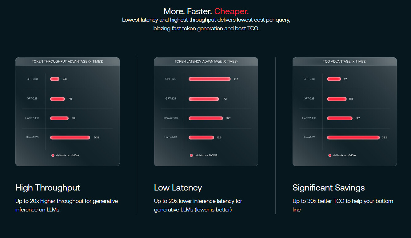
Intel Unleashes Enterprise AI with Gaudi 3, AI Open Systems Strategy and New Customer Wins

At the Intel Vision 2024 customer and partner conference, Intel introduced the Intel Gaudi 3 accelerator to bring performance, openness and choice to enterprise generative AI (GenAI), and unveiled a suite of new open scalable systems, next-gen products and strategic collaborations to accelerate GenAI adoption. With only 10% of enterprises successfully moving GenAI projects into production last year, Intel's latest offerings address the challenges businesses face in scaling AI initiatives.

"Innovation is advancing at an unprecedented pace, all enabled by silicon - and every company is quickly becoming an AI company," said Intel CEO Pat Gelsinger. "Intel is bringing AI everywhere across the enterprise, from the PC to the data center to the edge. Our latest Gaudi, Xeon and Core Ultra platforms are delivering a cohesive set of flexible solutions tailored to meet the changing needs of our customers and partners and capitalize on the immense opportunities ahead."

Intel Lunar Lake Chiplet Arrangement Sees Fewer Tiles—Compute and SoC

Intel Core Ultra "Lunar Lake-MX" will be the company's bulwark against Apple's M-series Pro and Max chips, designed to power the next crop of performance ultraportables. The MX codename extension denotes MoP (memory-on-package), which sees stacked LPDDR5X memory chips share the package's fiberglass substrate with the chip, to conserve PCB footprint, and give Intel greater control over the right kind of memory speed, timings, and power-management features suited to its microarchitecture. This is essentially what Apple does with its M-series SoCs powering its MacBooks and iPad Pros. Igor's Lab scored the motherlode on the way Intel has restructured the various components across its chiplets, and the various I/O wired to the package.

When compared to "Meteor Lake," the "Lunar Lake" microarchitecture sees a small amount of "re-aggregation" of the various logic-heavy components of the processor. On "Meteor Lake," the CPU cores and the iGPU sat on separate tiles—Compute tile and Graphics tile, respectively, with a large SoC tile sitting between them, and a smaller I/O tile that serves as an extension of the SoC tile. All four tiles sat on top of a Foveros base tile, which is essentially an interposer—a silicon die that facilitates high-density microscopic wiring between the various tiles that are placed on top of it. With "Lunar Lake," there are only two tiles—the Compute tile, and the SoC tile.

Arm Launches Next-Generation Neoverse CSS V3 and N3 Designs for Cloud, HPC, and AI Acceleration

Last year, Arm introduced its Neoverse Compute Subsystem (CSS) for the N2 and V2 series of data center processors, providing a reference platform for the development of efficient Arm-based chips. Major cloud service providers like AWS with Graviton 4 and Trainuium 2, Microsoft with Cobalt 100 and Maia 100, and even NVIDIA with Grace CPU and Bluefield DPUs are already utilizing custom Arm server CPU and accelerator designs based on the CSS foundation in their data centers. The CSS allows hyperscalers to optimize Arm processor designs specifically for their workloads, focusing on efficiency rather than outright performance. Today, Arm has unveiled the next generation CSS N3 and V3 for even greater efficiency and AI inferencing capabilities. The N3 design provides up to 32 high-efficiency cores per die with improved branch prediction and larger caches to boost AI performance by 196%, while the V3 design scales up to 64 cores and is 50% faster overall than previous generations.

Both the N3 and V3 leverage advanced features like DDR5, PCIe 5.0, CXL 3.0, and chiplet architecture, continuing Arm's push to make chiplets the standard for data center and cloud architectures. The chiplet approach enables customers to connect their own accelerators and other chiplets to the Arm cores via UCIe interfaces, reducing costs and time-to-market. Looking ahead, Arm has a clear roadmap for its Neoverse platform. The upcoming CSS V4 "Adonis" and N4 "Dionysus" designs will build on the improvements in the N3 and V3, advancing Arm's goal of greater efficiency and performance using optimized chiplet architectures. As more major data center operators introduce custom Arm-based designs, the Neoverse CSS aims to provide a flexible, efficient foundation to power the next generation of cloud computing.

Raytheon works with AMD to develop next-gen Multi-Chip Package

Raytheon, an RTX business, has been awarded a $20 million contract through the Strategic and Spectrum Missions Advanced Resilient Trusted Systems (S2MARTS) consortium to develop a next-generation multi-chip package for use in ground, maritime and airborne sensors. Under the contract, Raytheon will package state-of-the-art commercial devices from industry partners like AMD to create a compact microelectronics package that will convert radio frequency energy to digital information with more bandwidth and higher data rates. The integration will result in new system capabilities designed with higher performance, lower power consumption and reduced weight.

"By teaming with commercial industry, we can incorporate cutting-edge technology into Department of Defense applications on a much faster timescale," said Colin Whelan, president of Advanced Technology at Raytheon. "Together, we will deliver the first multi-chip package that features the latest in interconnect ability - which will provide new system capabilities to our warfighters."

Chinese Researchers Want to Make Wafer-Scale RISC-V Processors with up to 1,600 Cores

According to the report from a journal called Fundamental Research, researchers from the Institute of Computing Technology at the Chinese Academy of Sciences have developed a 256-core multi-chiplet processor called Zhejiang Big Chip, with plans to scale up to 1,600 cores by utilizing an entire wafer. As transistor density gains slow, alternatives like multi-chiplet architectures become crucial for continued performance growth. The Zhejiang chip combines 16 chiplets, each holding 16 RISC-V cores, interconnected via network-on-chip. This design can theoretically expand to 100 chiplets and 1,600 cores on an advanced 2.5D packaging interposer. While multi-chiplet is common today, using the whole wafer for one system would match Cerebras' breakthrough approach. Built on 22 nm process technology, the researchers cite exascale supercomputing as an ideal application for massively parallel multi-chiplet architectures.

Careful software optimization is required to balance workloads across the system hierarchy. Integrating near-memory processing and 3D stacking could further optimize efficiency. The paper explores lithography and packaging limits, proposing hierarchical chiplet systems as a flexible path to future computing scale. While yield and cooling challenges need further work, the 256-core foundation demonstrates the potential of modular designs as an alternative to monolithic integration. China's focus mirrors multiple initiatives from American giants like AMD and Intel for data center CPUs. But national semiconductor ambitions add urgency to prove domestically designed solutions can rival foreign innovation. Although performance details are unclear, the rapid progress shows promise in mastering modular chip integration. Combined with improving domestic nodes like the 7 nm one from SMIC, China could easily create a viable Exascale system in-house.

TSMC Plans to Put a Trillion Transistors on a Single Package by 2030

During the recent IEDM conference, TSMC previewed its process roadmap for delivering next-generation chip packages packing over one trillion transistors by 2030. This aligns with similar long-term visions from Intel. Such enormous transistor counts will come through advanced 3D packaging of multiple chipsets. But TSMC also aims to push monolithic chip complexity higher, ultimately enabling 200 billion transistor designs on a single die. This requires steady enhancement of TSMC's planned N2, N2P, N1.4, and N1 nodes, which are slated to arrive between now and the end of the decade. While multi-chipset architectures are currently gaining favor, TSMC asserts both packaging density and raw transistor density must scale up in tandem. Some perspective on the magnitude of TSMC's goals include NVIDIA's 80 billion transistor GH100 GPU—among today's largest chips, excluding wafer-scale designs from Cerebras.

Yet TSMC's roadmap calls for more than doubling that, first with over 100 billion transistor monolithic designs, then eventually 200 billion. Of course, yields become more challenging as die sizes grow, which is where advanced packaging of smaller chiplets becomes crucial. Multi-chip module offerings like AMD's MI300X and Intel's Ponte Vecchio already integrate dozens of tiles, with PVC having 47 tiles. TSMC envisions this expansion to chip packages housing more than a trillion transistors via its CoWoS, InFO, 3D stacking, and many other technologies. While the scaling cadence has recently slowed, TSMC remains confident in achieving both packaging and process breakthroughs to meet future density demands. The foundry's continuous investment ensures progress in unlocking next-generation semiconductor capabilities. But physics ultimately dictates timelines, no matter how aggressive the roadmap.

Ayar Labs Showcases 4 Tbps Optically-enabled Intel FPGA at Supercomputing 2023

Ayar Labs, a leader in silicon photonics for chip-to-chip connectivity, will showcase its in-package optical I/O solution integrated with Intel's industry-leading Agilex Field-Programmable Gate Array (FPGA) technology. In demonstrating 5x current industry bandwidth at 5x lower power and 20x lower latency, the optical FPGA - packaged in a common PCIe card form factor - has the potential to transform the high performance computing (HPC) landscape for data-intensive workloads such as generative artificial intelligence (AI), machine learning, and support novel new disaggregated compute and memory architectures and more.

"We're on the cusp of a new era in high performance computing as optical I/O becomes a 'must have' building block for meeting the exponentially growing, data-intensive demands of emerging technologies like generative AI," said Charles Wuischpard, CEO of Ayar Labs. "Showcasing the integration of Ayar Labs' silicon photonics and Intel's cutting-edge FPGA technology at Supercomputing is a concrete demonstration that optical I/O has the maturity and manufacturability needed to meet these critical demands."

Socionext Announces Collaboration with Arm and TSMC on 2nm Multi-Core Leading CPU Chiplet Development

Socionext today announced a collaboration with Arm and TSMC for the development of an innovative power-optimized 32-core CPU chiplet in TSMCʼs 2 nm silicon technology, delivering scalable performance for hyperscale data center server, 5/6G infrastructure, DPU and edge-of- network markets.

The engineering samples are targeted to be available in 1H2025. This advanced CPU chiplet proof-of-concept using Arm Neoverse CSS technology is designed for single or multiple instantiations within a single package, along with IO and application-specific custom chiplets to optimize performance for a variety of end applications.

Zero ASIC Democratizing Chip Making

Zero ASIC, a semiconductor startup, came out of stealth today to announce early access to its one-of-a-kind ChipMaker platform, demonstrating a number of world firsts:
  • 3D chiplet composability enabling billions of new silicon products
  • Fully automated no-code chiplet-based chip design
  • Zero install interactive RTL-based chip emulation
  • Roadmap to 100X reduction in chip development costs
"Custom Application Specific Integrated Circuits (ASICs) offer 10-100X cost and energy advantage over commercial off the shelf (COTS) devices, but the enormous development cost makes ASICs non-viable for most applications," said Andreas Olofsson, CEO and founder of Zero ASIC. "To build the next wave of world changing silicon devices, we need to reduce the barrier to ASICs by orders of magnitude. Our mission at Zero ASIC is to make ordering an ASIC as easy as ordering catalog parts from an electronics distributor."

JEDEC and Open Compute Project Foundation Pave the Way for a New Era of Chiplet Innovation

In an extraordinary leap forward for the chiplet industry, the groundbreaking collaboration between the Open Compute Project Foundation (OCP) and JEDEC is set to usher in a new era of innovation. By merging the capabilities and open standards of OCP's Chiplet Data Extensible Markup Language (CDXML) and JEDEC's JEP30 PartModel Guidelines, this partnership, initiated in late 2022, promises to revolutionize chiplet design, manufacturing and integration. The result will be a unified structure that supports both chiplets and general electronic parts within the overarching purview of JEDEC.

In a significant development, the integration of OCP CDXML into JEP30 has reached a critical milestone, enabling chiplet builders to provide standardized chiplet part descriptions to their customers electronically. This advancement opens the door to automating System in Package (SiP) design and assembly using chiplets. The chiplet descriptions encompass crucial information for SiP builders, including thermal properties, physical and mechanical requirements, behavior specifications, power and signal integrity properties, testing in-package and security parameters.

Tenstorrent Selects Samsung Foundry to Manufacture Next-Generation AI Chiplet

Tenstorrent, a company that sells AI processors and licenses AI and RISC-V IP, announced today that it selected Samsung Foundry to bring Tenstorrent's next generation of AI chiplets to market. Tenstorrent builds powerful RISC-V CPU and AI acceleration chiplets, aiming to push the boundaries of compute in multiple industries such as data center, automotive and robotics. These chiplets are designed to deliver scalable power from milliwatts to megawatts, catering to a wide range of applications from edge devices to data centers.

To ensure the highest quality and cutting-edge manufacturing capabilities for its chiplet, Tenstorrent has selected Samsung's Foundry Design Service team, known for their expertise in silicon manufacturing. The chiplets will be manufactured using Samsung's state-of-the-art SF4X process, which boasts an impressive 4 nm architecture.

TSMC Announces Breakthrough Set to Redefine the Future of 3D IC

TSMC today announced the new 3Dblox 2.0 open standard and major achievements of its Open Innovation Platform (OIP) 3DFabric Alliance at the TSMC 2023 OIP Ecosystem Forum. The 3Dblox 2.0 features early 3D IC design capability that aims to significantly boost design efficiency, while the 3DFabric Alliance continues to drive memory, substrate, testing, manufacturing, and packaging integration. TSMC continues to push the envelope of 3D IC innovation, making its comprehensive 3D silicon stacking and advanced packaging technologies more accessible to every customer.

"As the industry shifted toward embracing 3D IC and system-level innovation, the need for industry-wide collaboration has become even more essential than it was when we launched OIP 15 years ago," said Dr. L.C. Lu, TSMC fellow and vice president of Design and Technology Platform. "As our sustained collaboration with OIP ecosystem partners continues to flourish, we're enabling customers to harness TSMC's leading process and 3DFabric technologies to reach an entirely new level of performance and power efficiency for the next-generation artificial intelligence (AI), high-performance computing (HPC), and mobile applications."

NVIDIA Blackwell GB100 Die Could Use MCM Packaging

NVIDIA's upcoming Blackwell GPU architecture, expected to succeed the current Ada Lovelace architecture, is gearing up to make some significant changes. While we don't have any microarchitectural leaks, rumors are circulating that Blackwell will have different packaging and die structures. One of the most intriguing aspects of the upcoming Blackwell is the mention of a Multi-Chip Module (MCM) design for the GB100 data-center GPU. This advanced packaging approach allows different GPU components to exist on separate dies, providing NVIDIA with more flexibility in chip customization. This could mean that NVIDIA can more easily tailor its chips to meet the specific needs of various consumer and enterprise applications, potentially gaining a competitive edge against rivals like AMD.

While Blackwell's release is still a few years away, these early tidbits paint a picture of an architecture that isn't just an incremental improvement but could represent a more significant shift in how NVIDIA designs its GPUs. NVIDIA's potential competitor is AMD's upcoming MI300 GPU, which utilized chiplets in its designs. Chiplets also provide ease of integration as smaller dies provide better wafer yields, meaning that it makes more sense to switch to smaller dies and utilize chiplets economically.

Intel Unveils Industry-Leading Glass Substrates to Meet Demand for More Powerful Compute

What's New: Intel today announced one of the industry's first glass substrates for next-generation advanced packaging, planned for the latter part of this decade. This breakthrough achievement will enable the continued scaling of transistors in a package and advance Moore's Law to deliver data-centric applications.

"After a decade of research, Intel has achieved industry-leading glass substrates for advanced packaging. We look forward to delivering these cutting-edge technologies that will benefit our key players and foundry customers for decades to come."
-Babak Sabi, Intel senior vice president and general manager of Assembly and Test Development

d-Matrix Announces $110 Million in Funding for Corsair Inference Compute Platform

d-Matrix, the leader in high-efficiency generative AI compute for data centers, has closed $110 million in a Series-B funding round led by Singapore-based global investment firm Temasek. The goal of the fundraise is to enable d-Matrix to begin commercializing Corsair, the world's first Digital-In Memory Compute (DIMC), chiplet-based inference compute platform, after the successful launches of its prior Nighthawk, Jayhawk-I and Jayhawk II chiplets.

d-Matrix's recent silicon announcement, Jayhawk II, is the latest example of how the company is working to fundamentally change the physics of memory-bound compute workloads common in generative AI and large language model (LLM) applications. With the explosion of this revolutionary technology over the past nine months, there has never been a greater need to overcome the memory bottleneck and current technology approaches that limit performance and drive up AI compute costs.

QuickLogic & YorChip Collaborate on Development of Low-Power, Low-Cost UCIe FPGA Chiplets

QuickLogic Corporation, a developer of embedded FPGA (eFPGA) IP, ruggedized FPGAs and Endpoint AI/ML solutions, and YorChip, a pioneering startup specializing in UCIe-compatible IP, have formed a strategic partnership to revolutionize the world of FPGA chiplets. The collaboration will result in a groundbreaking lineup of FPGA chiplets optimized for low power consumption and low cost, opening new possibilities for a wide range of applications, including the fast-growing edge IoT and AI/ML markets.

According to Yole Group, a market research company, by 2023, they expect chiplet adoption will lead to a TAM of chiplet-based integrated circuits in excess of $200B, across the consumer, automotive defense, aerospace, industrial, and medical markets. Since discrete FPGAs are already prevalent in those same markets, wide adoption of eFPGA-based UCIe (Unified Chiplet Interconnect Express) enabled chiplets is expected, and QuickLogic and YorChip are well-positioned to capitalize on this growth opportunity.

AMD Radeon RX 7900 GRE ASIC Smaller than Navi 31, Slightly Larger than Navi 21

The GPU at the heart of the China-exclusive AMD Radeon RX 7900 GRE (Golden Rabbit Edition) sparked much curiosity. It is a physically different GPU from the one found in desktop Radeon RX 7900 XT and RX 7900 XTX graphics cards. AMD wouldn't go through all that effort designing a whole different GPU just for a limited edition graphics card, which means this silicon could find greater use for the company—for example, this could be the package AMD uses for its upcoming mobile RX 7900 series. AMD wouldn't go through all the effort designing a first-party MBA (made by AMD) PCB for the silicon just for the RX 7900 GRE, and so this PCB, with this particular version of the "Navi 31" silicon, could see a wider global launch, probably as the rumored Radeon RX 7800 XT, or something else (although with a different set of specs from the RX 7900 GRE).

We compared the sizes of the new "Navi 31" package found in the RX 7900 GRE, with those of the regular "Navi 31" powering the RX 7900 XT/XTX, the previous-generation "Navi 21" powering the RX 6900 XT, and the NVIDIA AD103 silicon powering the desktop GeForce RTX 4080. There are some interesting findings. The new smaller "Navi 31" package is visibly smaller than the one powering the RX 7900 XT/XTX. It is a square package, compared to the larger rectangular one, and has a significantly thinner metal reinforcement brace. What's interesting is that the 5 nm GCD is still surrounded by six 6 nm MCDs. We don't know if they've disabled two of the six MCDs, or whether they're dummies. AMD uses dummy chiplets as structural reinforcement in some of its EPYC server processors. The dummies spread some of the mounting pressure applied by the IHS or cooling solution, so the logic behind surrounding the GCD with six of these MCDs could be the same.

Silicon Box Opens US$2 Billion Advanced Semiconductor Assembly Plant in Singapore

Somewhat out of the blue, Silicon Box has announced the opening of its US$2 billion semiconductor assembly plant in Singapore. The "startup" is founded by several of Marvell's founders, suggesting the company has the right pedigree to compete in what is sure to be a very competitive market over the next few years. Silicon Box is not a foundry and will at least at this point in time, not be involved in foundry services, but instead the company will focus on advanced chip packaging technologies, focusing on chiplets.

The company is promising "faster time-to-market, lower new device design cost" on its very rudimentary website, something the company has yet to prove to be capable of. However, its new plant in Singapore covers 73,000 square metres and is said to feature state of the art production equipment for turning chiplets into chips. The factory is said to create some 1,200 jobs in Singapore, suggesting that this is a company that means business. According to a comment by company founder and CEO BJ Han to Reuters, "customers had been lining up" since before the completion of the assembly plant. Silicon Box is expecting to have several AI chipset companies as its customers, including Tenstorrent, which so far is the only officially mentioned client. Time will tell if Silicon Box can compete with established chip packaging businesses and if they can deliver on their promise to be faster and cheaper than the competition.

TSMC Certifies Ansys Multiphysics Solutions for TSMC's N2 Silicon Process

Ansys and TSMC continue their long-standing technology collaboration to announce the certification of Ansys' power integrity software for TSMC's N2 process technology. The TSMC N2 process, which adopts nanosheet transistor structure, represents a major advancement in semiconductor technology with significant speed and power advantages for high performance computing (HPC), mobile chips, and 3D-IC chiplets. Both Ansys RedHawk-SC and Ansys Totem are certified for power integrity signoff on N2, including the effects of self-heat on long-term reliability of wires and transistors. This latest collaboration builds on the recent certification of the Ansys platform for TSMC's N4 and N3E FinFLEX processes.

"TSMC works closely with our Open Innovation Platform (OIP) ecosystem partners to help our mutual customers achieve the best design results with the full stack of design solutions on TSMC's most advanced N2 process," said Dan Kochpatcharin, head of the Design Infrastructure Management Division at TSMC. "Our latest collaboration with Ansys RedHawk-SC and Totem analysis tools allows our customers to benefit from the significant power and performance improvements of our N2 technology while ensuring predictively accurate power and thermal signoff for the long-term reliability of their designs."

Intel Foundry and Arm Announce Multigeneration Collaboration on Leading-Edge SoC Design

Intel Foundry Services (IFS) and Arm today announced a multigeneration agreement to enable chip designers to build low-power compute system-on-chips (SoCs) on the Intel 18A process. The collaboration will focus on mobile SoC designs first, but allow for potential design expansion into automotive, Internet of Things (IoT), data center, aerospace and government applications. Arm customers designing their next-generation mobile SoCs will benefit from leading-edge Intel 18A process technology, which delivers new breakthrough transistor technologies for improved power and performance, and from IFS's robust manufacturing footprint that includes U.S.- and EU-based capacity.

"There is growing demand for computing power driven by the digitization of everything, but until now fabless customers have had limited options for designing around the most advanced mobile technology," said Pat Gelsinger, CEO of Intel Corporation. "Intel's collaboration with Arm will expand the market opportunity for IFS and open up new options and approaches for any fabless company that wants to access best-in-class CPU IP and the power of an open system foundry with leading-edge process technology."

Intel 14th Gen Core Lineup Confirmed to be Meteor Lake CPU Range

The Meteor Lake codename has been linked to the fourteenth generation of Intel's Core lineup for a while, following several significant leaks in 2022 and 2023. According to newly unearthed internal documentation and benchmark data, Intel has confirmed that the Meteor Lake family of CPUs will form its upcoming 14th Gen Core lineup - with laptop variations expected to arrive mid-2023 and heavily speculated desktop units in the fourth quarter, although a middle of the year refresh of Raptor Lake could push the entire Meteor Lake range's release window into 2024.

Meteor Lake is anticipated to be Intel's debuting of a "disaggregated" design - the most advanced laptop CPU variant features a top-of-the-line 6P+8E core configuration. Intel is solely responsible for fabrication of an IOE (I/O) tile (the company's own term for a chiplet) with PCIe 5.0 plus Thunderbolt 4, as well as an SoC tile. The GPU part of the design is rumored to be based on their own Arc Alchemist architecture, and TSMC has been contracted to manufacture this graphics tile - not a big surprise since Intel has also placed substantial manufacturing orders for discrete Arc cards with the Taiwanese foundry.
Return to Keyword Browsing
Apr 30th, 2024 19:55 EDT change timezone

New Forum Posts

Popular Reviews

Controversial News Posts