 830
830
NVIDIA GeForce GTX 480 Fermi Review
(830 Comments) »Introduction
Finally! Today NVIDIA releases their highly anticipated GeForce GTX 480 and GeForce GTX 470 cards. While the initial announcement of the Fermi architecture was back in 2009, the actual cards are being released just now.
NVIDIA has radically redesigned their GPU in order to bring maximum performance for DirectX 11 - especially tesselation. You can read more about the Fermi architecture here.
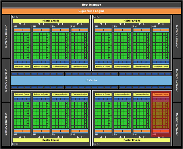
The specifications are certainly interesting. Instead of using all 512 shaders which are physically present inside the GPU, NVIDIA has chosen to disable one SM on the GTX 480 and two SMs on the GTX 470. I marked one SM red in the picture above, but it can be any one of the 16 that are present inside the GPU. As a result, NVIDIA's flagship GeForce GTX 480 comes with "only" 480 shaders. While unfortunate, this move makes NVIDIA's life much easier on several levels. First of all, they can build more cards out of the GPUs they get back from TSMC. Even if a slight defect is present in the silicon which would make some shaders unusable that chip can still be harvested into a shipping product. Another benefit is that the lower shader count reduces the power consumption of the card which affects heat and fan noise too. Last but not least it gives NVIDIA the option to release a higher performing Fermi-based single GPU card quickly if it should be needed.
It seems NVIDIA took a really good look at price/performance of their GeForce GTX 480 and positioned it properly so it can compete with AMD's HD 5870. Many people (including me) expected a price in the $600 range, or even above. So it comes as a relief to see the cards being offered at $499. At least that's NVIDIA's MSRP, the actual pricing in the market will also be dependant on supply and demand. While not officially confirmed we have heard the number 10,000 in regard to Fermi availability from company sources, so this means that everybody who wants a card can get one - hopefully. Also it should be noted that today there will be no cards available at e-tailers. Stock is expected to hit the shelves around mid-April.
| Radeon HD 4870 X2 | GeForce GTX 285 | Radeon HD 5850 | GeForce GTX 470 | Radeon HD 5870 | GeForce GTX 480 | GeForce GTX 295 | Radeon HD 5970 | |
| Shader units | 2x 800 | 240 | 1440 | 448 | 1600 | 480 | 2x 240 | 2x 1600 |
| ROPs | 2x 16 | 32 | 32 | 40 | 32 | 48 | 2x 28 | 2x 32 |
| GPU | 2x RV770 | GT200b | Cypress | GF100 | Cypress | GF100 | 2x GT200b | 2x Cypress |
| Transistors | 2x 956M | 1400M | 2154M | 3200M | 2154M | 3200M | 2x 1400M | 2x 2154M |
| Memory Size | 2x 1024 MB | 1024 MB | 1024 MB | 1215 MB | 1024 MB | 1536 MB | 2x 896 MB | 2x 1024 MB |
| Memory Bus Width | 2x 256 bit | 512 bit | 256 bit | 320 bit | 256 bit | 384 bit | 2x 448 bit | 2x 256 bit |
| Core Clock | 750 MHz | 648 MHz | 725 MHz | 607 MHz | 850 MHz | 700 MHz | 576 MHz | 725 MHz |
| Memory Clock | 900 MHz | 1242 MHz | 1000 MHz | 837 MHz | 1200 MHz | 924 MHz | 999 MHz | 1000 MHz |
| Price | $350 | $350 | $310 | $349 | $400 | $499 | $520 | $630 |
Packaging


NVIDIA handed out their sample cards at an event in Paris. We did not receive a retail packaging, but still a nice colorful box designed by NVIDIA that gives the product a much nicer first impression than just a card in an anti-static bag.
Our card came without bundle, but we hear that AIBs will be including Mini-HDMI to HDMI adapters, DVI to HDMI adapters and software like NVIDIA's Rocket Sled Demo or Car Garage.
The Card
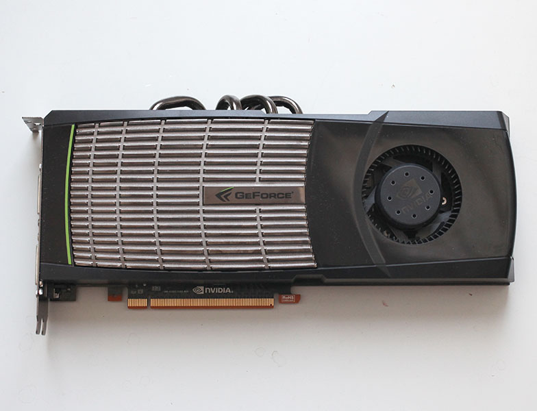

Unlike previous generations, this time there is no cover on the back of the card. It is not needed anyway since there are no components on that side that need cooling.
The front is covered by an intricate cooler design which we will cover in more detail on the next page.

The card occupies two slots in the system, which is what everyone expected. In my opinion a single slot design of this card is not possible without redesign of the GPU.

The card has two DVI ports and one one mini-HDMI port. According to NVIDIA the card also supports DisplayPort if board partners want to use it. Unlike AMD's latest GPUs, the output logic design is not as flexible. On AMD cards vendors are free to combine six TMDS links into any output configuration they want (dual-link DVI consuming two links), from what we know so far, on NVIDIA, you are fixed to two DVI outputs and one HDMI/DP in addition to that. NVIDIA confirmed that you can use only two displays at the same time, so for a three monitor setup you would need two cards.
NVIDIA has included an HDMI sound device inside their GPU which does away with the requirement of connecting an external audio source to the card for HDMI audio. The HDMI interface is HDMI 1.3a compatible which includes Dolby TrueHD, DTS-HD, AC-3, DTS and up to 7.1 channel audio with 192 kHz / 24-bit. NVIDIA also claims full support for the 3D portion of the HDMI 1.4 specification which will become important later this year when we will see first Blu-Ray titles shipping with support for 3D output.

You may combine two or three cards into SLI configurations for increased performance or image quality settings. Due to the high thermal requirements of these cards NVIDIA recommends that SLI configurations only be installed in certified cases that offer additional airflow for these setups.
It should also be noted that the retail boards come with a small piece of foam on the back of the card (will add pics once I have them). The foam acts as a spacer between multiple cards in SLI, so that there is a gap for the cooler to suck in enough air to keep the card cool. Also the gap helps avoid short circuits from the conductive metal surface of the cooler touching the back of the other card.


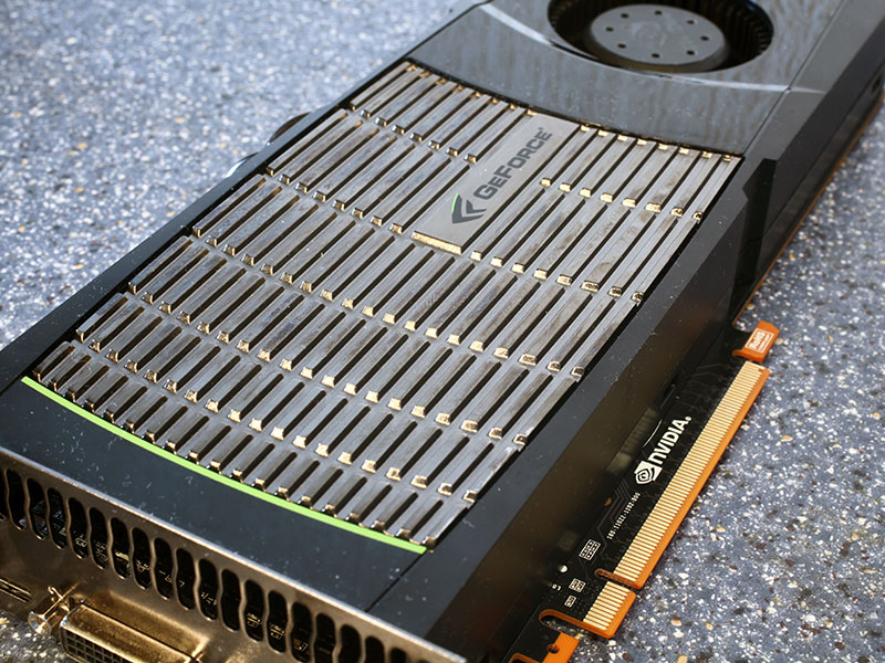
Here are the front and the back of the card, high-res versions are also available (front, back). If you choose to use these images for voltmods etc, please include a link back to this site or let us post your article.
A Closer Look

NVIDIA's thermal solution is a complex system that consists of several components that can be removed one after another. First we removed the black plastic shroud, this is done by pushing in a small number of clips near the cooler base.


The main function of the plastic shroud is to direct airflow and to provide physical protection for the components on the card. The design also looks like something that could be easily customized by add-in board vendors.


Once the shroud is gone, you can take a close look at the actual heatsink design. A large piece of metal with five heatpipes soaks up the heat from the GPU core and transports it to the cooling fins where it is dissipated in the airflow. Please also note that this cooler uses a direct touch heatpipe design that we have first seen on CPU coolers.


Once the GPU heatsink is gone you are left with a black metal piece that is responsible for cooling the other components of the card. This is the configuration that many watercoolers or extreme coolers will use. If you take a look at the thermal pads in the third picture you can easily spot the cooled components: memory and voltage regulation circuitry.
NVIDIA is using a Delta fan, which is rated at 1.8 A, whereas most GeForce GTX 200 fans are rated at 1.4 A. This seems to suggest that NVIDIA designed their cooling solution with bigger heatloads in mind.

NVIDIA uses a 6+8 pin power design which is certainly needed. According to NVIDIA the max. board power of the card is 250 W - our readings say more like 320 W. Either way, a dual 6-pin design wouldn't be possible as that design is specified for only 225 W maximum power draw.

The GDDR5 memory chips are made by Samsung, and carry the model number K4G10325FE-HC04. They are specified to run at 1250 MHz (5000 MHz GDDR5 effective). This is the first time that NVIDIA is using GDDR5 memory on a high-end card, while ATI has been using GDDR5 for years now.

Hey, that's something new. NVIDIA uses a CHiL CHL 8266 voltage regulator on their card. To be honest I have never heard of a company by that name until I saw it used on the GeForce GTX 480. Unfortunately there is not a lot of info available about that voltage regulator, but it is certain that it supports voltage adjustments via I2C.

NVIDIA's GeForce 100 graphics processor is made on a 40 nm process at TSMC Taiwan. It uses approximately 3.2 billion transistors which makes it the most complex GPU built to-date. Please note that the silvery metal surface you see is the heatspreader of the GPU which measures 42.3 x 42.3 mm. The actual GPU die is sitting under the heatspreader, its dimensions are not known. NVIDIA did not communicate a die size measurement to the press.
Our Patreon Silver Supporters can read articles in single-page format.
May 2nd, 2024 16:34 EDT
change timezone
Latest GPU Drivers
New Forum Posts
- Bad temps? (11)
- FINAL FANTASY XIV: Dawntrail Official Benchmark (74)
- 7800x3d $216 in bundle at Microcenter (19)
- AAF Optimus DCH Audio Modded Driver for Windows 10/11 - For ALL HDAUDIO Enumerator Chips (655)
- 7900 XTX Seriously lacking (105)
- What phone you use as your daily driver? And, a discussion of them. (1505)
- Ryzen Owners Zen Garden (7284)
- Aorus laptop 15p kd i7 11800h rtx 3060 (3)
- Post your Speedtest.net Speeds! (2257)
- Throttlestop stopped working (VBS is disabled) (4)
Popular Reviews
- Ugreen NASync DXP4800 Plus Review
- ASRock NUC BOX-155H (Intel Core Ultra 7 155H) Review
- Montech Sky Two GX Review
- HYTE THICC Q60 240 mm AIO Review
- Upcoming Hardware Launches 2023 (Updated Feb 2024)
- MOONDROP x Crinacle DUSK In-Ear Monitors Review - The Last 5%
- Team Group T-Force Vulcan ECO DDR5-6000 32 GB CL38 Review
- AMD Ryzen 7 7800X3D Review - The Best Gaming CPU
- Thermalright Phantom Spirit 120 EVO Review
- ASUS Radeon RX 7900 GRE TUF OC Review
Controversial News Posts
- Intel Statement on Stability Issues: "Motherboard Makers to Blame" (228)
- Windows 11 Now Officially Adware as Microsoft Embeds Ads in the Start Menu (159)
- Sony PlayStation 5 Pro Specifications Confirmed, Console Arrives Before Holidays (117)
- AMD's RDNA 4 GPUs Could Stick with 18 Gbps GDDR6 Memory (112)
- NVIDIA Points Intel Raptor Lake CPU Users to Get Help from Intel Amid System Instability Issues (106)
- AMD "Strix Halo" Zen 5 Mobile Processor Pictured: Chiplet-based, Uses 256-bit LPDDR5X (103)
- AMD Ryzen 9 7900X3D Now at a Mouth-watering $329 (102)
- TechPowerUp Hiring: Reviewers Wanted for Motherboards, Laptops, Gaming Handhelds and Prebuilt Desktops (93)