 332
332
NVIDIA GeForce GTX 580 1536 MB Review
(332 Comments) »GTX 580 Review Introduction
Enter the GeForce GTX 580 review. If two weeks ago somebody told us that today NVIDIA would be hard-launching a new high-end graphics processor under a new product family (the GeForce GTX 500 series), we'd have laughed out loud. We were too busy looking in AMD's direction for its new high-end GPU in the works, which is still nowhere in the horizon. It's that freaky moment in which you're slowly treading your way in a fairly linear horror FPS game, and turn around to find a monster breathing down on you. If the fact that NVIDIA was working on releasing a new high-end successor to the Fermi based GTX 480 today wasn't surprise enough, the fact the GeForce GTX 580 is claimed by NVIDIA to be the "best" GPU, and not just the fastest, certainly is. The GTX 480 gave us more than satisfactory performance, but was a bit of a let down on the thermals, and power consumption fronts. The claim that NVIDIA made the GeForce GTX 580 to outperform the GTX 480 and have better thermals and lower power draw certainly raises some eyebrows, because NVIDIA is building the GF110 GPU on a TSMC 40 nm process, just like the existing GF100 "Fermi".

NVIDIA's GF110 graphics processor is still based on the Fermi architecture and the GTX 580 review's architecture diagram looks exactly the same as the 512 shader GF100 version. However, GF110 can certainly be described as built from ground up. NVIDIA is said to have made improvements to GTX 580 key components at the level of transistors, making sure that there are lower latencies between components on the GPU, and electrical leakages are minimized. In GTX 580's 3 billion transistor chip that draws over 200W of power, leakages are the main enemy to power efficiency and overall chip stability. The GeForce GTX 580 packs 512 CUDA cores (up from 480 on the GeForce GTX 480), and features 64 texture memory units (TMUs), 48 raster operations processors (ROPs), and a 384-bit GDDR5 memory interface holding 1.5 GB of memory. The clock speeds are also upped from the previous generation, 772 MHz core, 1544 MHz CUDA cores, and 1002 MHz memory. The GTX 580 is capable of rendering 2 billion triangles per second (a staggering figure). Other than that there are no other major changes to the GeForce GTX 580 feature set.
| GeForce GTX 460 | GeForce GTX 460 | Radeon HD 6850 | Radeon HD 5850 | GeForce GTX 470 | Radeon HD 6870 | Radeon HD 5870 | GeForce GTX 480 | GeForce GTX 580 | Radeon HD 5970 | |
| Shader units | 336 | 336 | 960 | 1440 | 448 | 1120 | 1600 | 480 | 512 | 2x 1600 |
| ROPs | 24 | 32 | 32 | 32 | 40 | 32 | 32 | 48 | 48 | 2x 32 |
| GPU | GF104 | GF104 | Barts | Cypress | GF100 | Barts | Cypress | GF100 | GF110 | 2x Cypress |
| Transistors | 1950M | 1950M | 1700M | 2154M | 3200M | 1700M | 2154M | 3200M | 3000M | 2x 2154M |
| Memory Size | 768 MB | 1024 MB | 1024 MB | 1024 MB | 1280 MB | 1024 MB | 1024 MB | 1536 MB | 1536 MB | 2x 1024 MB |
| Memory Bus Width | 192 bit | 256 bit | 256 bit | 256 bit | 320 bit | 256 bit | 256 bit | 384 bit | 384 bit | 2x 256 bit |
| Core Clock | 675 MHz | 675 MHz | 775 MHz | 725 MHz | 607 MHz | 900 MHz | 850 MHz | 700 MHz | 772 MHz | 725 MHz |
| Memory Clock | 900 MHz | 900 MHz | 1000 MHz | 1000 MHz | 837 MHz | 1050 MHz | 1200 MHz | 924 MHz | 1002 MHz | 1000 MHz |
| Price | $160 | $200 | $180 | $260 | $260 | $240 | $360 | $450 | $500 | $580 |
The Card


NVIDIA's card looks more like a GeForce GTX 285 card than a GTX 480. NVIDIA has implemented several changes to the cooler which certainly help the card keep cooler than GTX 480. Also there is an extra space around the fan opening to allow for easier access to air when running in SLI.

NVIDIA's GeForce GTX 580 requires two slots in your system.

The card has two DVI ports and one one mini-HDMI port. According to NVIDIA the card also supports DisplayPort if board partners want to use it. Unlike AMD's latest GPUs, the output logic design is not as flexible. On AMD cards vendors are free to combine six TMDS links into any output configuration they want (dual-link DVI consuming two links), on NVIDIA, you are fixed to two DVI outputs and one HDMI/DP in addition to that. NVIDIA confirmed that you can use only two displays at the same time, so for a three monitor setup you would need two cards.
NVIDIA has included an HDMI sound device inside their GPU which does away with the requirement of connecting an external audio source to the card for HDMI audio. The HDMI interface is HDMI 1.3a compatible which includes Dolby TrueHD, DTS-HD, AC-3, DTS and up to 7.1 channel audio with 192 kHz / 24-bit. NVIDIA also claims full support for the 3D portion of the HDMI 1.4 specification which will become important later this year when we will see first Blu-Ray titles shipping with support for 3D output.

You may combine up to four GeForce GTX 580 cards in SLI for increased performance or improved image quality settings.


Here are the front and the back of the card, high-res versions are also available (front, back). If you choose to use these images for voltmods etc, please include a link back to this site or let us post your article.
A Closer Look


The GeForce GTX 580 is one of the few graphics cards that uses a vapor-chamber technology heatplate to maximize heat transfer between the GPU and the rest of the heatsink. You can also see above that the heatsink cools secondary components like voltage regulation circuitry and memory chips. Overall this seems to be a very capable thermal solution but that also increases its price.

NVIDIA's 6+8 power input configuration is sufficient for the GTX 580 design and provides up to 300 W.
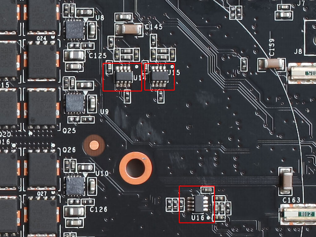

In order to stay within the 300 W power limit, NVIDIA has added a power draw limitation system to their card. When either Furmark or OCCT are detected running by the driver, three Texas Instruments INA219 sensors measure the inrush current and voltage on all 12 V lines (PCI-E slot, 6-pin, 8-pin) to calculate power. As soon as the power draw exceeds a predefined limit, the card will automatically clock down and restore clocks as soon as the overcurrent situation has gone away. NVIDIA emphasizes this is to avoid damage to cards or motherboards from these stress testing applications and claims that in normal games and applications such an overload will not happen. At this time the limiter is only engaged when the driver detects Furmark / OCCT, it is not enabled during normal gaming. NVIDIA also explained that this is just a work in progress with more changes to come. From my own testing I can confirm that the limiter only engaged in Furmark and OCCT and not in other games I tested. I am still concerned that with heavy overclocking, especially on water and LN2 the limiter might engage, and reduce clocks which results in reduced performance. Real-time clock monitoring does not show the changed clocks, so besides the loss in performance it could be difficult to detect that state without additional testing equipment or software support.
I did some testing of this feature in Furmark and recorded card only power consumption over time. As you can see the blue line fluctuates heavily over time which also affects clocks and performance accordingly. Even though we see spikes over 300 W in the graph, the average (represented by the purple line) is clearly below 300 W. It also shows that the system is not flexible enough to adjust power consumption to hit exactly 300 W.

The GDDR5 memory chips are made by Samsung, and carry the model number K4G10325FE-HC04. They are specified to run at 1250 MHz (5000 MHz GDDR5 effective).
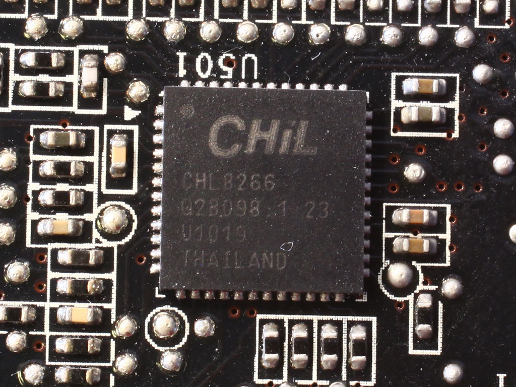
Just like on the GeForce GTX 480, NVIDIA uses a CHiL CHL 8266 voltage regulator on their card. This controller offers extensive monitoring and voltage control options via I2C, so it's a great choice for overclockers.

NVIDIA's GeForce 110 graphics processor is made on a 40 nm process at TSMC Taiwan. It uses approximately 3.0 billion transistors which is 200 million less than the GF100. Please note that the silvery metal surface you see is the heatspreader of the GPU. The actual GPU die is sitting under the heatspreader, its dimensions are not known. According to NVIDIA, the die size of the GF110 graphics processor is 520 mm².
Test System
| Test System - VGA Rev. 11 | |
|---|---|
| CPU: | Intel Core i7 920 @ 3.8 GHz (Bloomfield, 8192 KB Cache) |
| Motherboard: | Gigabyte X58 Extreme Intel X58 & ICH10R |
| Memory: | 3x 2048 MB Mushkin Redline XP3-12800 DDR3 @ 1520 MHz 8-7-7-16 |
| Harddisk: | WD Caviar Black 6401AALS 640 GB |
| Power Supply: | akasa 1200W |
| Software: | Windows 7 64-bit |
| Drivers: | GTX 580: 262.99 old NVIDIA cards: 258.96 HD 6800: Catalyst 10.10 HD 5970: Catalyst 10.10c old ATI cards: Catalyst 10.7 |
| Display: | LG Flatron W3000H 30" 2560x1600 |
- All video card results were obtained on this exact system with the exact same configuration.
- All games were set to their highest quality setting
- 1024 x 768, No Anti-aliasing. This is a standard resolution without demanding display settings.
- 1280 x 1024, 2x Anti-aliasing. Common resolution for most smaller flatscreens today (17" - 19"). A bit of eye candy turned on in the drivers.
- 1680 x 1050, 4x Anti-aliasing. Most common widescreen resolution on larger displays (19" - 22"). Very good looking driver graphics settings.
- 1920 x 1200, 4x Anti-aliasing. Typical widescreen resolution for large displays (22" - 26"). Very good looking driver graphics settings.
- 2560 x 1600, 4x Anti-aliasing. Highest possible resolution for commonly available displays (30"). Very good looking driver graphics settings.
Our Patreon Silver Supporters can read articles in single-page format.
May 6th, 2024 01:04 EDT
change timezone
Latest GPU Drivers
New Forum Posts
- How to check flatness of CPUs and coolers - INK and OPTICAL INTERFERENCE methods (113)
- Trouble Getting Vega Rig Running (0)
- Apparently Valve is giving refunds on Helldivers 2 regardless of hour count. Details inside. (81)
- Overheating/undervolt/setup issues (3)
- Only some humans can see refresh rates faster than others, I am one of those humans. (142)
- Free Games Thread (3781)
- TPU's WCG/BOINC Team (34421)
- What software are you using to monitor CPU temps during gaming session? (21)
- Alphacool CORE 1 CPU block - bulging with danger of splitting? (101)
- Current Sales, Bundles, Giveaways (10227)
Popular Reviews
- Finalmouse UltralightX Review
- ASRock NUC BOX-155H (Intel Core Ultra 7 155H) Review
- Meze Audio LIRIC 2nd Generation Closed-Back Headphones Review
- Cougar Hotrod Royal Gaming Chair Review
- Upcoming Hardware Launches 2023 (Updated Feb 2024)
- Montech Sky Two GX Review
- AMD Ryzen 7 7800X3D Review - The Best Gaming CPU
- HYTE THICC Q60 240 mm AIO Review
- ASUS Radeon RX 7900 GRE TUF OC Review
- Logitech G Pro X Superlight 2 Review - Updated with 4000 Hz Tested
Controversial News Posts
- Intel Statement on Stability Issues: "Motherboard Makers to Blame" (240)
- Windows 11 Now Officially Adware as Microsoft Embeds Ads in the Start Menu (167)
- AMD to Redesign Ray Tracing Hardware on RDNA 4 (156)
- Sony PlayStation 5 Pro Specifications Confirmed, Console Arrives Before Holidays (117)
- AMD's RDNA 4 GPUs Could Stick with 18 Gbps GDDR6 Memory (114)
- NVIDIA Points Intel Raptor Lake CPU Users to Get Help from Intel Amid System Instability Issues (106)
- AMD Ryzen 9 7900X3D Now at a Mouth-watering $329 (104)
- AMD "Strix Halo" Zen 5 Mobile Processor Pictured: Chiplet-based, Uses 256-bit LPDDR5X (103)