News Posts matching #Samsung

Return to Keyword Browsing

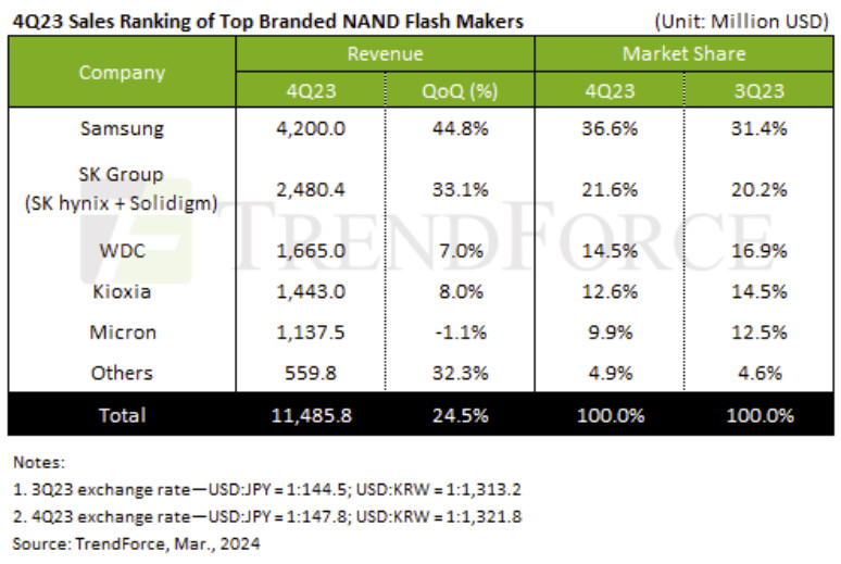
NAND Flash Industry Revenue Grows 24.5% in Q4 2023, Expected to Increase Another 20% in Q1

TrendForce reports a substantial 24.5% QoQ increase in NAND Flash industry revenue, hitting US$11.49 billion in 4Q23. This surge is attributed to a stabilization in end-demand spurred by year-end promotions, along with an expansion in component market orders driven by price chasing, leading to robust bit shipments compared to the same period last year. Additionally, the corporate sector's continued positive outlook for 2024 demand—compared to 2023—and strategic stockpiling have further fueled this growth.

Looking ahead to 1Q24, despite it traditionally being an off-season, the NAND Flash industry is expected to see a continued increase in revenue by another 20%. This anticipation is underpinned by significant improvements in supply chain inventory levels and ongoing price rises, with clients ramping up their orders to sidestep potential supply shortages and escalating costs. The ongoing expansion of order sizes is expected to drive NAND Flash contract prices up by an average of 25%.

Samsung Foundry Renames 3 nm Process to 2 nm Amid Competition with Intel

In a move that could intensify competition with Intel in the cutting-edge chip manufacturing space, Samsung Foundry has reportedly decided to rebrand its second-generation 3 nm-class fabrication technology, previously known as SF3, to a 2 nm-class manufacturing process called SF2. According to reports from ZDNet, the renaming of Samsung's SF3 to SF2 is likely an attempt by the South Korean tech giant to simplify its process nomenclature and better compete against Intel Foundry, at least visually. Intel is set to roll out its Intel 20A production node, a 2 nm-class technology, later this year. The reports suggest that Samsung has already notified its customers about the changes in its roadmap and the renaming of SF3 to SF2. Significantly, the company has reportedly gone as far as re-signing contracts with customers initially intended to use the SF3 production node.

"We were informed by Samsung Electronics that the 2nd generation 3 nm [name] is being changed to 2 nm," an unnamed source noted to ZDNet. "We had contracted Samsung Foundry for the 2nd generation 3 nm production last year, but we recently revised the contract to change the name to 2 nm." Despite the name change, Samsung's SF3, now called SF2, has not undergone any actual process technology alterations. This suggests that the renaming is primarily a marketing move, as using a different process technology would require customers to rework their chip designs entirely. Samsung intends to start manufacturing chips based on the newly named SF2 process in the second half of 2024. The SF2 technology, which employs gate-all-around (GAA) transistors that Samsung brands as Multi-Bridge-Channel Field Effect Transistors (MBCFET), does not feature a backside power delivery network (BSPDN), a significant advantage of Intel's 20A process. Samsung Foundry has not officially confirmed the renaming.

JEDEC Publishes GDDR7 Graphics Memory Standard

JEDEC Solid State Technology Association, the global leader in the development of standards for the microelectronics industry, is pleased to announce the publication of JESD239 Graphics Double Data Rate (GDDR7) SGRAM. This groundbreaking new memory standard is available for free download from the JEDEC website. JESD239 GDDR7 offers double the bandwidth over GDDR6, reaching up to 192 GB/s per device, and is poised to meet the escalating demand for more memory bandwidth in graphics, gaming, compute, networking and AI applications.

JESD239 GDDR7 is the first JEDEC standard DRAM to use the Pulse Amplitude Modulation (PAM) interface for high frequency operations. Its PAM3 interface improves the signal to noise ratio (SNR) for high frequency operation while enhancing energy efficiency. By using 3 levels (+1, 0, -1) to transmit 3 bits over 2-cycles versus the traditional NRZ (non-return-to-zero) interface transmitting 2 bits over 2-cycles, PAM3 offers higher data transmission rate per cycle resulting in improved performance.

DRAM Industry Sees Nearly 30% Revenue Growth in 4Q23 Due to Rising Prices and Volume

TrendForce reports a 29.6% QoQ in DRAM industry revenue for 4Q23, reaching US$17.46 billion, propelled by revitalized stockpiling efforts and strategic production control by leading manufacturers. Looking ahead to 1Q24, the intent to further enhance profitability is evident, with a projected near 20% increase in DRAM contract prices—albeit with a slight decrease in shipment volumes to the traditional off-season.

Samsung led the pack with the highest revenue growth among the top manufacturers in Q4 as it jumped 50% QoQ to hit $7.95 billion, largely due to a surge in 1alpha nm DDR5 shipments, boosting server DRAM shipments by over 60%. SK hynix saw a modest 1-3% rise in shipment volumes but benefited from the pricing advantage of HBM and DDR5, especially from high-density server DRAM modules, leading to a 17-19% increase in ASP and a 20.2% rise in revenue to $5.56 billion. Micron witnessed growth in both volume and price, with a 4-6% increase in each, resulting in a more moderate revenue growth of 8.9%, totaling $3.35 billion for the quarter due to its comparatively lower share of DDR5 and HBM.

Samsung's New microSD Cards Bring High Performance and Capacity, with Speeds of up to 800 MB/s and 1 TB in Size

Samsung Electronics, the world leader in advanced memory technology, today announced that it has started sampling its 256-gigabyte (GB) SD Express microSD card with sequential read speed of up to 800 megabytes per second (MB/s) and has commenced mass production of its 1-terabyte (TB) UHS-1 microSD card. With the introduction of its next-generation microSD card line-up, Samsung aims to provide differentiated memory solutions required for tomorrow's mobile computing and on-device AI applications.

"With our two new microSD cards, Samsung has provided effective solutions to address the growing demands of mobile computing and on-device AI," said Hangu Sohn, Vice President of the Memory Brand Product Biz Team at Samsung Electronics. "Despite their tiny size, these memory cards deliver powerful SSD-like performance and capacity to help users get more out of demanding modern and future applications."

Samsung & Intel Discuss the Galaxy Book4 Series and Future of AI PCs

Samsung Electronics is making 2024 the year of the AI PC with the release of its most powerful and intelligent Galaxy Book product line yet, the Galaxy Book4 series. This latest lineup—consisting of the Galaxy Book4 Ultra, Galaxy Book4 Pro and Galaxy Book4 Pro 360—offers intelligent performance, enhanced security and a vivid, interactive display, all in an ultra-portable design. From the new Intel Core Ultra Processor to the suite of AI features, the Galaxy Book4 series is packed with cutting-edge technology that aims to not only simplify but amplify users' computing experience.

Visitors discovered the Galaxy Book4 series' full capabilities inside Samsung's booth at Mobile World Congress (MWC) 2024, the world's largest mobile exhibition held from February 26-29 in Barcelona, Spain. Samsung Newsroom sat down with Mincheol Lee, Head of Galaxy Eco Biz Team, Mobile eXperience Business at Samsung Electronics, and David Feng, Vice President of Client Computing Group and General Manager of Client Segments at Intel, to explore how the advancements in the Galaxy Book4 series can enrich the lives of users.

Samsung Develops Industry-First 36GB HBM3E 12H DRAM

Samsung Electronics, a world leader in advanced memory technology, today announced that it has developed HBM3E 12H, the industry's first 12-stack HBM3E DRAM and the highest-capacity HBM product to date. Samsung's HBM3E 12H provides an all-time high bandwidth of up to 1,280 gigabytes per second (GB/s) and an industry-leading capacity of 36 gigabytes (GB). In comparison to the 8-stack HBM3 8H, both aspects have improved by more than 50%.

"The industry's AI service providers are increasingly requiring HBM with higher capacity, and our new HBM3E 12H product has been designed to answer that need," said Yongcheol Bae, Executive Vice President of Memory Product Planning at Samsung Electronics. "This new memory solution forms part of our drive toward developing core technologies for high-stack HBM and providing technological leadership for the high-capacity HBM market in the AI era."

Samsung Electronics Joins AI-RAN Alliance as a Founding Member

Samsung Electronics announced that it is participating in the AI-RAN Alliance as a founding member, with the goal of promoting 6G innovation by combining AI technology and wireless communication technology. Officially launched at Mobile World Congress (MWC) Barcelona 2024 today, the AI-RAN Alliance is an organization aimed at revitalizing the convergence of AI and wireless communication and leading technology innovation through cooperation with related companies. A total of eleven organizations—including Samsung, Arm, Ericsson, Microsoft, Nokia, NVIDIA, SoftBank and Northeastern University—are participating as founding members. This new alliance will collaborate on the development of innovative new technologies, as well as the application of these technologies to commercial products in preparation for the upcoming 6G era.

"Emerging services in the 6G era will revolutionize the way people interact with technology, and AI will be an integral part of this trend," said Charlie Zhang, Senior Vice President at Samsung Research America. "The AI-RAN Alliance will foster collaboration, drive innovation and usher in a new era of transformation around AI and 6G networks. We believe this coalition will create new value for end users and operators through AI-based use cases and innovations."

Samsung Collaborates on vRAN 3.0 with Intel

Samsung Electronics today announced the company has successfully completed the industry's first end-to-end call in a lab environment with a future Intel Xeon processor (codenamed Granite Rapids-D), on a virtualized Open RAN network powered by Samsung's vRAN 3.0. This achievement between Samsung and Intel is another milestone in the companies' multi-year collaboration and represents the companies' mutual dedication to advance virtualized Open RAN for enhanced performance and capacity.

Conducted in Samsung's R&D lab in Korea, the companies completed the end-to-end data call using Samsung's versatile and O-RAN-compliant virtualized RAN (vRAN) integrated with Intel's Granite Rapids-D, Samsung's Core and test devices. During the test, Samsung achieved significant gains as well as reduced power consumption. The test results will be demonstrated at Mobile World Congress 2024 (Samsung Networks booth, invitation-only).

Supermicro Accelerates Performance of 5G and Telco Cloud Workloads with New and Expanded Portfolio of Infrastructure Solutions

Supermicro, Inc. (NASDAQ: SMCI), a Total IT Solution Provider for AI, Cloud, Storage, and 5G/Edge, delivers an expanded portfolio of purpose-built infrastructure solutions to accelerate performance and increase efficiency in 5G and telecom workloads. With one of the industry's most diverse offerings, Supermicro enables customers to expand public and private 5G infrastructures with improved performance per watt and support for new and innovative AI applications. As a long-term advocate of open networking platforms and a member of the O-RAN Alliance, Supermicro's portfolio incorporates systems featuring 5th Gen Intel Xeon processors, AMD EPYC 8004 Series processors, and the NVIDIA Grace Hopper Superchip.

"Supermicro is expanding our broad portfolio of sustainable and state-of-the-art servers to address the demanding requirements of 5G and telco markets and Edge AI," said Charles Liang, president and CEO of Supermicro. "Our products are not just about technology, they are about delivering tangible customer benefits. We quickly bring data center AI capabilities to the network's edge using our Building Block architecture. Our products enable operators to offer new capabilities to their customers with improved performance and lower energy consumption. Our edge servers contain up to 2 TB of high-speed DDR5 memory, 6 PCIe slots, and a range of networking options. These systems are designed for increased power efficiency and performance-per-watt, enabling operators to create high-performance, customized solutions for their unique requirements. This reassures our customers that they are investing in reliable and efficient solutions."

Samsung Foundry Reportedly Producing 2 nm Prototypes for Qualcomm

Smartphone chipset industry watchdogs believe that the Samsung 3 nm GAA process did not meet customer expectations, due to alleged yield issues. TSMC is seemingly victorious in this segment, as reports suggest that a next-generation 3 nm node production goal of "100,000 monthly wafers by the end of 2024" has been set. Three days ago, Samsung Foundry revealed that it is working on a very advanced SF2 GAAFET process—press outlets in South Korea propose that the manufacturing giant is hoping to outmuscle its main rival in a future 2 nm node category. Tuesday's press introduction stated that a development partnership is set: "to deliver optimized next generation ARM Cortex -X CPU developed on Samsung Foundry's latest Gate-All-Around (GAA) process technology."

A Sedaily article posits that the company's cutting-edge manufacturing tech has already attracted interest from notable parties: "Samsung Electronics is taking advantage of these advantages to win orders for the 2 nm project. Samsung Electronics took its first step by winning an order to produce a 2 nm AI accelerator from Preferred Networks (PFN), Japan's largest AI company. Qualcomm, the world's largest system semiconductor design company, has entered into discussions with Samsung Electronics' System LSI Division, which designs high-performance chips, to produce 2 nm prototypes." December 2023 news reports suggested that Samsung leadership was considering a 2 nm wafer price discount—in order to stay competitive with competing foundry services. It is possible that Qualcomm is evaluating the 2 nm SF2 GAAFET process for a distant Snapdragon 8 "Gen 5" chipset, while Samsung LSI could be working on a 2 nm "Exynos 2600" SoC design.

Samsung's New Galaxy Book4 Series Available Globally Beginning February 26

Samsung Electronics today announced the Galaxy Book4 series will be available in selected markets starting February 26. The latest premium PC lineup from Samsung delivers intelligent and powerful experiences that bring together highly optimized performance, a vivid touchscreen display and enhanced connectivity. The Galaxy Book4 series, including the Galaxy Book4 Ultra, Galaxy Book4 Pro and Galaxy Book4 Pro 360, launched in Korea on January 2 and experienced record-breaking interest, outselling last year's Galaxy Book3 series by 1.5 times during the first week of sales.

"We're excited for users to experience the intelligence, connectivity and productivity made possible by the Galaxy Book4 series, taking our premium PC lineup to the next level," said TM Roh, President and Head of Mobile eXperience Business at Samsung Electronics. "The Galaxy Book4 series delivers the powerful performance and multi-device connectivity that consumers expect from a high-performance PC in today's market."

Insiders Predict Slimmer Profiles on 2024 iPad Pro OLED Models

Mid-January reportage indicated that LG and Samsung plants in South Korea had commenced construction of next-gen Apple iPad OLED parts—while expert analysis has predicted a second quarter launch of 11 and 13-inch "Pro" tablet models. Omdia—an independent analyst and consultancy firm—has compiled its Apple field research into a forecasted roadmap of various portable products. Company analysts believe that: "LG Display (LGD) and Samsung Display (SDC) are preparing to mass-produce RGB tandem stack and Hybrid OLEDs from their half-Gen 6 fabs. Apple also plans to launch the MacBook Pro with OLED displays in 2026. BOE, LGD, and SDC are preparing their fab investments to produce RGB tandem stack and hybrid OLEDs at half-Gen 8.7 fabs."

9to5Mac's insider network detected whispers of possible Apple tablet physical profile adjustments—suggesting that a larger next-gen iPad Air is in the pipeline, alongside a thinner iPad Pro design update: "(we) first reported last year that Apple has been working on two new versions of the iPad Air, codenamed J507 and J537. While one of these models will look pretty much like the current iPad Air, the other will have a larger display. If true, this will be the first time Apple will offer the iPad Air in two different sizes. And according to our sources, this larger iPad Air will have essentially the same dimensions as the current 12.9-inch iPad Pro, suggesting that the screen size will also be almost identical. The smaller iPad Air is unlikely to have any significant design changes."

Samsung and Square Enix Ready SSD 990 PRO x FFVII Rebirth Collector's Edition

Samsung is partnering with Square Enix to launch a limited collector's edition package of the 990 PRO 2 TB SSD co-branded with Final Fantasy VII Rebirth (FFVII Rebirth). The package consists of a special 180 mm x 180 mm x 175 mm (WxDxH) cuboidal box with branding and imagery from FFVII Rebirth characters. Inside, you'll find a Samsung 990 PRO 2 TB M.2 NVMe SSD with its reference heatsink. The heatsink makes the drive compatible with the PlayStation 5. There are no changes in the specs of the drive—it offers 2 TB of storage with a 2 GB LPDDR4 DRAM cache, and transfer speeds of up to 7450 MB/s sequential reads, and up to 6950 MB/s sequential writes, making it among the fastest Gen 4 SSDs in the market. But that's it with the bundle—you don't actually get the game, but a special edition box that can make for a good background prop if you're streaming. The limited collector's edition is expected to come out some time in March 2024.

Samsung Electronics Collaborates with Arm on Optimized Next Gen Cortex-X CPU Using 2nm SF2 GAAFET Process

Samsung Electronics Co., Ltd., a world leader in advanced semiconductor technology, today announced a collaboration to deliver optimized next generation Arm Cortex -X CPU developed on Samsung Foundry's latest Gate-All-Around (GAA) process technology. This initiative is built on years of partnership with millions of devices shipped with Arm CPU intellectual property (IP) on various process nodes offered by Samsung Foundry.

This collaboration sets the stage for a series of announcements and planned innovation between Samsung and Arm. The companies have bold plans to reinvent 2-nanometer (nm) GAA for next-generation data center and infrastructure custom silicon, and a groundbreaking AI chiplet solution that will revolutionize the future generative artificial intelligence (AI) mobile computing market.

Samsung & Vodafone "Open RAN Ecosystem" Bolstered by AMD EPYC 8004 Series

Samsung Electronics and Vodafone, in collaboration with AMD, today announced that the three companies have successfully demonstrated an end-to-end call with the latest AMD processors enabling Open RAN technology, a first for the industry. This joint achievement represents the companies' technical leadership in enriching the Open RAN ecosystem throughout the industry. Conducted in Samsung's R&D lab in Korea, the first call was completed using Samsung's versatile, O-RAN-compliant, virtualized RAN (vRAN) software, powered by AMD EPYC 8004 Series processors on Supermicro's Telco/Edge servers, supported by Wind River Studio Container-as-a-Service (CaaS) platform. This demonstration aimed to verify optimized performance, energy efficiency and interoperability among partners' solutions.

The joint demonstration represents Samsung and Vodafone's ongoing commitment to reinforce their position in the Open RAN market and expand their ecosystem with industry-leading partners. This broader and growing Open RAN ecosystem helps operators to build and modernize mobile networks with greater flexibility, faster time-to-market (TTM), and unmatched performance. "Open RAN represents the forthcoming major transformation in advancing mobile networks for the future. Reaching this milestone with top industry partners like Samsung and AMD shows Vodafone's dedication to delivering on the promise of Open RAN innovation," said Nadia Benabdallah, Network Strategy and Engineering Director at Vodafone Group. "Vodafone is continually looking to innovate its network by exploring the potential and diversity of the ecosystem."

Samsung Bags 2 nm Wafer Order from Japanese AI Chip Startup

Samsung Electronics foundry has reportedly bagged a mass production order for its cutting edge 2 nm EUV foundry node from Japanese AI chip startup PFN (Preferred Networks). This is reportedly the first major third party order for the 2 nm node. Founded in 2014, PFN specializes in AI and IoT chips, and spun off from Preferred Infrastructure. Samsung's 2 nm node, called the SF2, is on track for delivery of mass produced chips in 2025, which means much of 2024 will be spent on testing, validation, and risk production, with the node expected to go live toward the end of the year. Samsung SF2 is being designed to offer 25% higher power efficiency (at iso-clocks), and 12% increase in performance, over SF3 (3 nm EUV FinFET). In the semiconductor fabrication market, Samsung SF2 competes against TSMC N2 and Intel 20A.

Samsung Announces the Galaxy Tab Active5

Samsung Electronics America has announced the Galaxy Tab Active5, a business-ready ruggedized tablet built to handle the rigors of frontline work. Building on the power of the Galaxy Tab Active3, the Galaxy Tab Active5 delivers significant improvements in performance, durability and security to help businesses conquer their challenges and boost productivity in the field, even in harsh working environments. Additionally, the Galaxy Tab Active5 is available as an Enterprise Edition, making it easy for businesses to enroll, configure, manage and analyze hundreds of devices.

Designed with the needs of retailers in mind, the Galaxy Tab Active5 features a high-resolution camera, near-field communication (NFC) and push-to-talk functionality to enable more efficient barcode-scanning, mobile point-of-sale (mPOS), in-store communication and more. In addition to retail, the Galaxy Tab Active5 also delivers new capabilities in other industries that require a high degree of durability, including foodservice, manufacturing, transportation, construction and the public sector.

NVIDIA to Create AI Semi-custom Chip Business Unit

NVIDIA is reportedly working to set up a new business unit focused on designing semi-custom chips for some of its largest data-center customers, Reuters reports. NVIDIA dominates the AI HPC processor market, although even its biggest customers are having to shop from its general lineup of A100 series and H100 series HPC processors. There are reports of some of these customers venturing out of the NVIDIA fold, wanting to develop their own AI processor designs. It is to cater to exactly this segment that NVIDIA is setting up the new unit.

A semi-custom chip isn't just a bespoke chip designed to a customer's specifications. It is co-developed by NVIDIA and its customer, using mainly NVIDIA IP blocks, but also integrating some third-party IP blocks the customer may want; and more importantly, approach semiconductor fabrication companies such as TSMC, Samsung, or Intel Foundry Services as separate entities from NVIDIA for their wafer allocation. For example, a company like Google may have a certain amount of wafer pre-allocation with TSMC (eg: for its Tensor SoCs powering the Pixel smartphones), which it may want to tap into for a semi-custom AI HPC processor for its cloud business. NVIDIA assesses a $30 billion TAM for this specific business unit—that's all its current customers wanting to pursue their own AI processor projects, who will now be motivated to stick to NVIDIA.

Interposer and Fan-out Wafer Level Packaging Market worth $63.5 billion by 2029: MarketsandMarkets Research

The global interposer and FOWLP market is expected to be valued at USD 35.6 billion in 2024 and is projected to reach USD 63.5 billion by 2029; it is expected to grow at a CAGR of 12.3% during the forecast period according to a new report by MarketsandMarkets. The increasing demand for advanced packaging in AI and high-performance computing (HPC) are the key drivers fueling the expansion of the interposer and FOWLP market.

Interposer-based packaging is experiencing robust growth in the semiconductor industry, leveraging its ability to enhance performance and reduce power consumption by facilitating efficient connections between diverse chip components. This technology is increasingly adopted for its role in enabling high-bandwidth and high-performance applications, driving advancements in data centers, 5G infrastructure, and emerging technologies.

Windows 11 DirectML Preview Supports Intel Core Ultra NPUs

Chad Pralle, Principle Technical Program Manager at Microsoft's Windows AI NPU division has introduced the DirectML 1.13.1 and ONNX Runtime 1.17 APIs—this appears to be a collaborative effort—Samsung was roped in to some degree, according to Microsoft's announcement and a recent Team Blue blog entry. Pralle and his team are suitably proud of this joint effort that involved open source models: "we are excited to announce developer preview support for NPU acceleration in DirectML, the machine learning platform API for Windows. This developer preview enables support for a subset of models on new Windows 11 devices with Intel Core Ultra processors with Intel AI boost."

Further on in Microsoft's introductory piece, Samsung Electronics is announced as a key launch partner—Hwang-Yoon Shim, VP and Head of New Computing H/W R&D Group stated that: "NPUs are emerging as a critical resource for broadly delivering efficient machine learning experiences to users, and Windows DirectML is one of the most efficient ways for Samsung's developers to make those experiences for Windows." Microsoft notes that NPU support in DirectML is still "a work in progress," but Pralle and his colleagues are eager to receive user feedback from the testing community. It is currently "only compatible with a subset of machine learning models, some models may not run at all or may have high latency or low accuracy." They hope to implement improvements in the near future. The release is limited to modern Team Blue hardware, so NPU-onboard AMD devices are excluded at this point in time, naturally.

Samsung Lands Significant 2 nm AI Chip Order from Unnamed Hyperscaler

This week in its earnings call, Samsung announced that its foundry business has received a significant order for a two nanometer AI chips, marking a major win for its advanced fabrication technology. The unnamed customer has contracted Samsung to produce AI accelerators using its upcoming 2 nm process node, which promises significant gains in performance and efficiency over today's leading-edge chips. Along with the AI chips, the deal includes supporting HBM and advanced packaging - indicating a large-scale and complex project. Industry sources speculate the order may be from a major hyperscaler like Google, Microsoft, or Alibaba, who are aggressively expanding their AI capabilities. Competition for AI chip contracts has heated up as the field becomes crucial for data centers, autonomous vehicles, and other emerging applications. Samsung said demand recovery in 2023 across smartphones, PCs and enterprise hardware will fuel growth for its broader foundry business. It's forging ahead with 3 nm production while eyeing 2 nm for launch around 2025.

Compared to its 3 nm process, 2 nm aims to increase power efficiency by 25% and boost performance by 12% while reducing chip area by 5%. The new order provides validation for Samsung's billion-dollar investments in next-generation manufacturing. It also bolsters Samsung's position against Taiwan-based TSMC, which holds a large portion of the foundry market share. TSMC landed Apple as its first 2 nm customer, while Intel announced 5G infrastructure chip orders from Ericsson and Faraday Technology using its "Intel 18A" node. With rivals securing major customers, Samsung is aggressively pricing 2 nm to attract clients. Reports indicate Qualcomm may shift some flagship mobile chips to Samsung's foundry at the 2 nm node, so if the yields are good, the node has a great potential to attract customers.

TSMC Overtakes Intel and Samsung to Become World's Largest Semiconductor Maker by Revenue

Taiwan Semiconductor Manufacturing Company (TSMC) has reached a significant milestone, overtaking Intel and Samsung to become the world's largest semiconductor maker by revenue. According to Taiwanese financial analyst Dan Nystedt, TSMC earned $69.3 billion in revenue in 2023, surpassing Intel's $63 billion and Samsung's $58 billion. This is a remarkable achievement for the Taiwanese chipmaker, which has historically lagged behind Intel and Samsung in terms of revenue despite being the world's largest semiconductor foundry. TSMC's meteoric rise has been fueled by the increased demand for everything digital - from PCs to game consoles - during the coronavirus pandemic in 2020, and AI demand in the previous year. With its cutting-edge production capabilities allowing it to manufacture chips using the latest process technologies, TSMC has pulled far ahead of Intel and Samsung and can now charge a premium for its services.

This is reflected in its financials. For the 6th straight quarter, TSMC's Q4 2023 revenue of $19.55 billion also beat Intel's $15.41 billion and Samsung's $16.42 billion chip division revenue. As the world continues its rapid transformation in the AI era of devices, TSMC looks set to hold on to its top position for the foreseeable future. Its revenue and profits will likely continue to eclipse those of historical giants like Intel and Samsung. However, a big contender is Intel Foundry Services, which is slowly starting to gain external customers. If IFS takes off and new customers start adopting Intel as their foundry of choice, team blue could regain leadership in the coming years.

Global Monitor Market Set for Recovery in 2024, with Shipments Projected to Increase by 2%

TrendForce's latest findings reveal global monitor shipments declined 7.3% in 2023 down to 125 million units—a figure below pre-pandemic levels. Looking ahead to 2024, given the low shipment base in 2023, alongside the potential for a gradual economic recovery and the typical 4 to 5-year PC replacement cycle, PCs purchased during the pandemic are expected to be upgraded between the second half of 2024 and 2025. This is anticipated to drive a 2% increase in global monitor shipments in 2024, reaching approximately 128 million units.

The top three commercial monitor brands experienced over twenty percent decline in shipments
A surge in unfulfilled business orders in Europe and America in the first half of 2022 elevated the shipment baseline for commercial brands that year. However, by 2023, commercial market demand saw a significant contraction, leading to a YoY shipment decrease of 20.4% for Dell, 20.7% for HP, and 21.4% for Lenovo—each dropping by over twenty percent.

Qualcomm & Samsung Sign Extended Multi-year Snapdragon Deal

Cristiano Renno Amon, President and CEO of Qualcomm, discussed the successful launch of his company's Snapdragon 8 Gen 3 mobile platform during a January 31 Earnings Call—expectations have been set high for the flagship smartphone chipset: "(bringing) a new standard for on-device gen AI experiences for premium smartphones and powers all through flagship Android devices launched and launching this fiscal year." Amon highlighted Samsung's recently rolled out Galaxy S24 Ultra range, that makes use of a special "For Galaxy" Snapdragon 8 Gen 3 SoC. Industry watchdogs have continued to question Samsung's reliance on third-party processor solutions (including MediaTek Dimensity parts), despite having access to plenty of "worthy" in-house technology. Their flagship Exynos 2400 chip has been deployed with the Galaxy S24 Plus range, but Qualcomm Snapdragon-equipped devices offer better performance and efficiency.

The picky segment of Samsung's smartphone userbase will be pleased to hear about a renewed agreement between it and Qualcomm, which includes a trickling down to mid-range offerings—Amon made a big announcement during the late January conference call: "We're also announcing that we extended a multi-year agreement with Samsung relating to Snapdragon platforms for flagship Galaxy smartphone launches starting in 2024. The extended agreement demonstrates the value of Snapdragon 8, our technology leadership and our successful long-term strategic partnership with Samsung. In the quarter, we also announced the Snapdragon 7 Gen 3 mobile platform, which brings leading gen AI capabilities to high-tier Android smartphones and is a category leader in both experiences and performance." Going forward, Samsung is likely sticking with its current operating model of peppering a mix of Snapdragon and Exynos chipsets throughout its Galaxy Z, S and A product ranges.
Return to Keyword Browsing
Jun 1st, 2024 13:15 EDT change timezone

New Forum Posts

Popular Reviews

Controversial News Posts