Report an Error


NVIDIA GP102
GP102

GP102-350-K1-A1

GP102-350-K2-A1

GP102-350-K3-A1

GP102-350-K4-A1

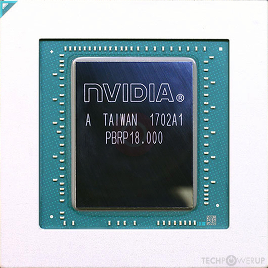
GP102-351-K1-A1

GP102-400-A1

GP102-450-A1

Fritzchens Fritz
Die Shot

Block Diagram

SM Diagram
NVIDIA's GP102 GPU uses the Pascal architecture and is made using a 16 nm production process at TSMC. With a die size of 471 mm² and a transistor count of 11,800 million it is a very big chip. GP102 supports DirectX 12 (Feature Level 12_1). For GPU compute applications, OpenCL version 3.0 and CUDA 6.1 can be used. It features 3840 shading units, 240 texture mapping units and 96 ROPs.
Graphics Processor
- Released
- Aug 2nd, 2016
- GPU Name
- GP102
- Codename
- NV132
- Architecture
- Pascal
- Foundry
- TSMC
- Process Size
- 16 nm
- Transistors
- 11,800 million
- Density
- 25.1M / mm²
- Die Size
- 471 mm²
- Package
- BGA-2397
Graphics Features
- DirectX
- 12 (12_1)
- OpenGL
- 4.6
- OpenCL
- 3.0
- Vulkan
- 1.3
- CUDA
- 6.1
- Shader Model
- 6.7
- WDDM
- 3.1
- NVENC
- 6th Gen
- NVDEC
- 3rd Gen
- PureVideo HD
- VP8
- VDPAU
- Feature Set H
Render Config
- Shading Units
- 3840
- TMUs
- 240
- ROPs
- 96
- SM Count
- 30
- SFUs
- 960
- TPCs
- 30
- GPCs
- 6
- L1 Cache
- 48 KB per SM
- L2 Cache
- 3072 KB
- Max. TDP
- 250 W
All Pascal GPUs
NVIDIA GPU Architecture History
- 2024 Blackwell
- 2023 Hopper
- 2022-2024 Ada Lovelace
- 2020-2024 Ampere
- 2018-2022 Turing
- 2017-2020 Volta
- 2016-2021 Pascal
- 2014-2019 Maxwell 2.0
- 2014-2017 Maxwell
- 2013-2015 Kepler 2.0
- 2012-2018 Kepler
- 2010-2016 Fermi 2.0
- 2010-2013 VLIW Vec4
- 2010-2016 Fermi
- 2007-2013 Tesla 2.0
- 2006-2010 Tesla
- 2003-2013 Curie
- 2003-2005 Rankine
- 2001-2003 Kelvin
- 1999-2005 Celsius
- 1998-2000 Fahrenheit
Graphics cards using the NVIDIA GP102 GPU
| Name | Chip | Memory | Shaders | TMUs | ROPs | Base Clock | Boost Clock | Memory Clock |
|---|---|---|---|---|---|---|---|---|
| GP102-400-A1 | 12 GB | 3584 | 224 | 96 | 1417 MHz | 1531 MHz | 1251 MHz | |
| GP102-875-A1 | 24 GB | 3840 | 240 | 96 | 1506 MHz | 1645 MHz | 1127 MHz | |
| GP102-350-K1-A1 | 11 GB | 3584 | 224 | 88 | 1481 MHz | 1582 MHz | 1376 MHz | |
| 24 GB | 3840 | 240 | 96 | 1303 MHz | 1531 MHz | 1808 MHz | ||
| GP102-450-A1 | 12 GB | 3840 | 240 | 96 | 1405 MHz | 1582 MHz | 1426 MHz | |
| GP102-100-A1 | 5 GB | 3200 | 200 | 80 | 1582 MHz | 1683 MHz | 1376 MHz | |
| GP102-101-A1 | 10 GB | 3200 | 200 | 80 | 1557 MHz | 1670 MHz | 2002 MHz | |
| 10 GB | 3200 | 200 | 80 | 1557 MHz | 1670 MHz | 1376 MHz | ||
| 24 GB | 3840 | 240 | 96 | 1025 MHz | 1493 MHz | 1808 MHz | ||
| 12 GB | 3200 | 200 | 80 | 1557 MHz | 1670 MHz | 1376 MHz |


GP102 GPU Notes
| NVENC: 6th Gen NVDEC: 3rd Gen PureVideo HD: VP8 VDPAU: Feature Set H Latest Drivers: Windows 7 / 8 / 8.1 (x32 / x64): GeForce Release 391.35 / 474.89 Quadro Release R390 U9 (392.37) / R440 U4 (441.66) Data Center Release 427.11 Windows 10 / 11 (x32 / x64): GeForce Release 391.35 / Latest Quadro Release R390 U9 (392.37) / Latest Data Center Release: Latest |
May 25th, 2024 07:45 EDT
change timezone
Latest GPU Drivers
New Forum Posts
- The TPU UK Clubhouse (24799)
- sysbench file IO benchmark (0)
- Gigabyte am5 motherboard ddr5 not posting when rebooting (24)
- Help! Black Screen When I Close Certain Games (R9 290) (24)
- Nvflash with PCI Subsystem ID mismatch disabled for linux (1)
- Can u use same tube of thermal paste? (17)
- 5800x (and other Zen 3 chips) PBO settings/Temperature fix (940)
- Air makes its way from the reservoir into the radiator. (85)
- [SOLVED] Can anyone ID this fan? (prop only, no markings - super challenge!) (32)
- Windows as a Service (WaaS) is coming. (28)
Popular Reviews
- Senua's Saga: Hellblade II Performance Benchmark Review
- Lian Li O11 Dynamic EVO XL Review
- Ghost of Tsushima Performance Benchmark Review - 35 GPUs Tested
- Ghost of Tsushima: DLSS vs. FSR vs. XeSS Comparison Review
- Granzon GAI0.1 CPU Water Block Review
- Upcoming Hardware Launches 2024 (Updated May 2024)
- PMG Audio Apx In-Ear Monitors Review - $6500 Flagship!
- CHERRY XTRFY M68 Pro Review
- Chieftec Apex Q Review
- Quick Look: Huion Kamvas Pro 24 (4K) Graphics Tablet
Controversial News Posts
- Intel Statement on Stability Issues: "Motherboard Makers to Blame" (272)
- AMD to Redesign Ray Tracing Hardware on RDNA 4 (227)
- NVIDIA to Only Launch the Flagship GeForce RTX 5090 in 2024, Rest of the Series in 2025 (154)
- AMD Hits Highest-Ever x86 CPU Market Share in Q1 2024 Across Desktop and Server (140)
- AMD RDNA 5 a "Clean Sheet" Graphics Architecture, RDNA 4 Merely Corrects a Bug Over RDNA 3 (139)
- AMD Ryzen 9 7900X3D Now at a Mouth-watering $329 (104)
- Core Configurations of Intel Core Ultra 200 "Arrow Lake-S" Desktop Processors Surface (101)
- Superior Stability by GIGABYTE BETA BIOS with Intel Baseline on Z790/B760 Motherboards (90)