Tuesday, June 5th 2018

AMD Demonstrates 7nm Radeon Vega Instinct HPC Accelerator
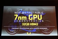
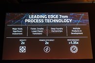
AMD demonstrated the world's first GPU built on the 7 nanometer silicon fabrication process, a Radeon Vega Instinct HPC/AI accelerator, with a 7 nm GPU based on the "Vega" architecture, at its heart. This chip is an MCM of a 7 nm GPU die, and 32 GB HBM2 memory stacks over four stacks (4096-bit memory bus width). It's also the first product to feature a removable InfinityFabric interface (competition to NVIDIA's NVLink interface). There will also be variants based on the common PCI-Express 3.0 x16. The card supports hardware virtualization and new deep-learning ops.


100 Comments on AMD Demonstrates 7nm Radeon Vega Instinct HPC Accelerator
If this chip clocks at 1200 MHz but only hits 1080ti performance after the 1100 series is out, it will be another flop, because having 1200mhz doesnt matter if the chip cant deliver. And after the 300, 400, 500, and vega series, I'm not holding my breath that AMD is going to compete well.
This chip looks promising, but so did vega 64, and we all saw how that went. If this new chip is only 1080ti level, my 480 replacement will most likely have to be an nvidia chip instead of an AMD chip, and I like my 480, so I'd prefer another AMD GPU.
To this day I can't figure out, if Vega is so great, why hasn't it turned into a mid-range SKU to crush both the GTX 1060 and the RX480/580.
Video RAM is sensitive to bandwidth much more than it is to latency.
The choice between HBM2, GDDR5 or GDDR5X is not about performance. Given the right combination of speed and bus width they can all get similar enough results.
Considerations are about cost, space on PCB/interposer, power consumption etc.That depends on what frequency we are talking about. The frequency at which you can request data from GDDR5(X) and HBM is actually (roughly) the same. GDDR5(X) can just transfer a lot of data back a lot (8-16 times) faster than it can be requested (per pin or effectively per same width of memory bus).
At least that's my understanding/guess about what previous posters were trying to say.
The spec used across different types is data transfer rate per pin (per each bit of memory bus).
When we are talking about bandwidth, that is simple. When we are talking about latency, it gets more complicated. While the actual memory reads are in the same range (actual DRAM clock speeds should remain around 1 GHz), word sizes differ - 16b/32b/64b for GDDR5(X) and 128b/256b for HBM2 - as well as addressing and read delays. I do not remember reading anything indepth about that and testing this is not too easy.
Take these three cards for example:
- Vega 64: gaming.radeon.com/en/product/vega/radeon-rx-vega-64/
- GTX 1080Ti: www.nvidia.com/en-us/geforce/products/10series/geforce-gtx-1080-ti/
- RX 580: www.amd.com/en/products/graphics/radeon-rx-580
Vega 64 (HBM2):
Memory Data Rate: 1.89Gbps
Memory Speed: 945MHz
Memory Interface: 2048-bit
Memory Bandwidth: Up to 484GB/s
945MHz memory on 2048-bit memory bus. Memory data rate is 1.89Gbps - 945MHz at dual data rate
Memory bandwidth is up to 484 GB/s = 1.89 Gbps x 2048 bits of bus / 8 bits per byte
GTX 1080Ti (GDDR5X):
Memory Speed: 11 Gbps
Memory Interface Width: 352-bit
Memory Bandwidth (GB/sec): 484
Memory bandwidth is up to 484 GB/s = 11 Gbps x 352 bits of bus / 8 bits per byte
Note that they do not list the memory clock in specs. Memory speed is actually the data rate spec. This is because there are multiple clocks for GDDR5(X) and none of these are exactly descriptive in a simple way. Knowing what the memory does, lets see what we can deduce about speeds.
GDDR5X is either dual or quad data rate, so at maximum I/O bus is running at quarter of the data rate - 11Gbps / 4 = 2.75 GHz
Data is being requested and read at a quarter of the I/O bus frequency (thanks to 16n prefetch) - 2.75 GHz / 4 = 0.687 GHz
Prefetch on GDDR5 means that where the memory needs to transfer out 32 bits of data at a time, it can internally load 8 (or 16 for GDDR5X) times as much from DRAM into prefetch buffers and for the next 8 (or 16) transfers send data from the buffer instead of going and loading up more data.
RX580 (GDDR5):
Memory speed (effective): 8 Gbps
Memory Interface: 256-bit
Max. Memory Bandwidth: 256 GB/s
Memory bandwidth is up to 256 GB/s = 8 Gbps x 256 bits of bus / 8 bits per byte
Again, memory speed is actually the data rate spec.
GDDR5 is also dual data rate, so I/O bus is running at half the data rate - 8 Gbps / 2 = 4 GHz
Data is being requested and read at a quarter of the I/O bus frequency (thanks to 8n prefetch) - 4 GHz / 4 = 1 GHz
community.amd.com/thread/229155
So stop dreaming :-D
It might be wise to distinguish between theoretical specs and actual performance. Just look at:
Vega 64: 4096 cores, 10215 GFlop/s, 483.8 GB/s.
GTX 1080: 2560 cores, 8228 GFlop/s, 320.2 GB/s.
I wonder which one performs better…
Compared to:
GTX 1080 Ti: 3584 cores, 10609 GFlop/s, 484.3 GB/s.
As we all know, Vega 64 have resources comparable to GTX 1080 Ti, so it's not the lack of resources like many AMD fans claim, but the lack of proper resource management.
In conclusion, theoretical specs might be similar on paper, but their actual performance will depend on the complete design.If I may add, memory latency is substantial, for DDR it's 50-60 ns for access, even more for GDDR. When you're talking of speeds of 1000 MHz and above, the latency factor becomes negligible, and higher clocks more or less just impacts the bandwidth.AMD have said all along that Vega 20 is targeting the "professional" market.
AMD can certainly change their mind, but as of this moment their position is still unchanged. But why would they bring Vega 20 to the consumer market? It only scales well with simple comute workloads, and Vega 20 is a GPU built for full fp64 support, which have no relevance for consumers.
www.tomshardware.com/reviews/radeon-r9-290x-hawaii-review,3650-29.html
Oh wait, silly me, it was offering performance at an affordable price: www.techpowerup.com/reviews/AMD/R9_290X/29.html
Though to be honest the 280 and 285 were really good cards. But 290X was clearly pushed beyond that architecture's sweet spot.
But your point is right; this might be the last "good shrink" for a long time. Moving an inefficient to a new node will not make it great, and since the competition will also move to the new node, the gap is only going to increase.
You see people arguing that a shrunk Vega will matter, but we know it wouldn't even come close to Pascal in efficiency. AMD isn't even planning a consumer Vega on 7 nm.
I was strictly talking about the "Moving an inefficient to a new node will not make it great" part - it will not make it great, but maybe that's not the point. Though God knows what AMD is thinking.
Zen has been a huge win but it came with compromises over pure performance in the PC enthusiast space, like low clocks/minimal overclocking and latency. The node is a big factor but Zen cores could have been designed for more performance at higher energy consumption and increased die space. AMD specifically said it wanted to make a core that could scale all the way from very low-wattage mobile to high-performance. That's nice but the word "scale" isn't a magic wand that erases the benefit of having more targeted designs. Those cost more money, though, to make and usually involve more risk. The key with Zen was to do just enough and keep it affordable. The high efficiency of the SMT was really a big design win, which is a bit droll considering its bet on CMT previously.
Gaming enthusiasts also are competing with AI/science/workstation/supercomputing, crypto, the laptop space, "consoles", etc. AMD wants one core that can do it all but what we would like is a special core for each niche — like a big core x86 with a loose library for high performance instead of just bigger core count. If AMD were bigger and richer it could do more of that. Crypto is probably more of a target for AMD's designers than gaming, outside of the console space. Crypto seems to fit better with the AI/science/workstation/supercomputing "pro compute" area. And, it, not PC gaming, holds the promise of demand higher than supply.
I wonder, for CPUs, if Big-Little will become a desktop trend. It seems to offer the benefits of turbo to a greater degree. Create several more powerful cores and supplement them with smaller ones. I'm sure articles have been written on this. But, maybe we'll someday see a desktop CPU with two large high-performance cores surrounded by smaller ones. Of course, like the enthusiast-grade gaming GPU, the enthusiast gamer x86 CPU seems to be mostly a thing of the past — or an afterthought at best. What advantage do those two big cores have for servers, for instance? I suppose it could be useful for some pro markets, though, like financial analysis (e.g. high-speed trading). With that, though, I don't see why supercomputers can't be harnessed. Is it really necessary to focus on a high-clock micro for those systems? Is the latency that bad?