- Joined
- Oct 9, 2007
- Messages
- 47,235 (7.55/day)
- Location
- Hyderabad, India
| System Name | RBMK-1000 |
|---|---|
| Processor | AMD Ryzen 7 5700G |
| Motherboard | ASUS ROG Strix B450-E Gaming |
| Cooling | DeepCool Gammax L240 V2 |
| Memory | 2x 8GB G.Skill Sniper X |
| Video Card(s) | Palit GeForce RTX 2080 SUPER GameRock |
| Storage | Western Digital Black NVMe 512GB |
| Display(s) | BenQ 1440p 60 Hz 27-inch |
| Case | Corsair Carbide 100R |
| Audio Device(s) | ASUS SupremeFX S1220A |
| Power Supply | Cooler Master MWE Gold 650W |
| Mouse | ASUS ROG Strix Impact |
| Keyboard | Gamdias Hermes E2 |
| Software | Windows 11 Pro |
ASUS has just designed a new monster graphics card that breaks the mold for reference design GeForce GTX 295, called the ASUS MARS 295 Limited Edition. The card, although retains the name "GeForce GTX 295", same device ID, and is compatible with existing NVIDIA drivers, has two huge innovations put in by ASUS, which go far beyond being yet another overclocked GeForce GTX 295: the company used two G200-350-B3 graphics processors, the same ones that make the GeForce GTX 285. The GPUs have all the 240 shader processors enabled, and also have the complete 512-bit GDDR3 memory interface enabled. This dual-PCB monstrosity holds 32 memory chips, and 4 GB of total memory (each GPU accesses 2 GB of it). Apart from these, each GPU system uses the same exact clock speeds as the GeForce GTX 285: 648/1476/2400 MHz (core/shader/memory).

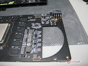
Each PCB holds 16 memory chips, a 6-phase digital PWM power circuit, drawing auxiliary power from an 8-pin PCI-E power connector, the GeForce GTX 285-class GPU, and its companion NVIO2 processor. The PCB holding the PCI-Express bus interface, also holds the bridge chip. ASUS broke away with using the nForce 200 chip, and instead is using a yet to be disclosed third-party bridge chip. Currently, PLX and IDT are two likely sources for such a chip. The memory consists of high-density 0.77 ns memory chips made by Hynix.


The electrical-management on each PCB is care of a Volterra VRM controller, which supports the I2C interface, which means that the card supports software voltage control, perhaps a big plus for ASUS' Voltage Tweak feature that is gaining in popularity. Fused power circuit provides Over Current Protection while also facilitating extreme overclocking.

The cooler internally has the same basic construction as the reference cooler, it uses a single leaf-blower. The card spans across two expansion slots and is slightly higher than the reference design card. ASUS also used slightly longer internal bridges that make more room for third-party coolers, and the likes. Our source from ASUS EMEA conducted a quick 3DMark Vantage test proving the card's seamless compatibility with existing drivers, while also providing a significant boost in performance over existing GTX 295 cards. Being Quad-SLI capable, this card finally makes GeForce GTX 285 (effective) quad-SLI possible, and makes for the most powerful desktop multi-GPU setup ever conceived. ASUS designed this card despite pressure from NVIDIA enforcing its rigid policy of restricting its partners from custom-designing GeForce GTX 295. If everything goes smooth throughout the development process, the card might make it for a gala launch at Computex.


View at TechPowerUp Main Site

Each PCB holds 16 memory chips, a 6-phase digital PWM power circuit, drawing auxiliary power from an 8-pin PCI-E power connector, the GeForce GTX 285-class GPU, and its companion NVIO2 processor. The PCB holding the PCI-Express bus interface, also holds the bridge chip. ASUS broke away with using the nForce 200 chip, and instead is using a yet to be disclosed third-party bridge chip. Currently, PLX and IDT are two likely sources for such a chip. The memory consists of high-density 0.77 ns memory chips made by Hynix.


The electrical-management on each PCB is care of a Volterra VRM controller, which supports the I2C interface, which means that the card supports software voltage control, perhaps a big plus for ASUS' Voltage Tweak feature that is gaining in popularity. Fused power circuit provides Over Current Protection while also facilitating extreme overclocking.


The cooler internally has the same basic construction as the reference cooler, it uses a single leaf-blower. The card spans across two expansion slots and is slightly higher than the reference design card. ASUS also used slightly longer internal bridges that make more room for third-party coolers, and the likes. Our source from ASUS EMEA conducted a quick 3DMark Vantage test proving the card's seamless compatibility with existing drivers, while also providing a significant boost in performance over existing GTX 295 cards. Being Quad-SLI capable, this card finally makes GeForce GTX 285 (effective) quad-SLI possible, and makes for the most powerful desktop multi-GPU setup ever conceived. ASUS designed this card despite pressure from NVIDIA enforcing its rigid policy of restricting its partners from custom-designing GeForce GTX 295. If everything goes smooth throughout the development process, the card might make it for a gala launch at Computex.


View at TechPowerUp Main Site
Last edited by a moderator:


