- Joined
- Oct 9, 2007
- Messages
- 47,243 (7.55/day)
- Location
- Hyderabad, India
| System Name | RBMK-1000 |
|---|---|
| Processor | AMD Ryzen 7 5700G |
| Motherboard | ASUS ROG Strix B450-E Gaming |
| Cooling | DeepCool Gammax L240 V2 |
| Memory | 2x 8GB G.Skill Sniper X |
| Video Card(s) | Palit GeForce RTX 2080 SUPER GameRock |
| Storage | Western Digital Black NVMe 512GB |
| Display(s) | BenQ 1440p 60 Hz 27-inch |
| Case | Corsair Carbide 100R |
| Audio Device(s) | ASUS SupremeFX S1220A |
| Power Supply | Cooler Master MWE Gold 650W |
| Mouse | ASUS ROG Strix Impact |
| Keyboard | Gamdias Hermes E2 |
| Software | Windows 11 Pro |
Intel Corporation and Micron Technology, Inc. today announced the world's first 25-nanometer (nm) NAND technology, which provides a more cost-effective path for increasing storage capacity in such popular consumer gadgets as smartphones, personal music and media players (PMPs), as well as the new high-performance class of solid-state drives (SSDs).
NAND flash memory stores data and other media contained in consumer electronics products, retaining information even when the power is turned off. The drive toward smaller NAND processes enables the continued development and introduction of new uses for the technology. Not only is the 25nm process the smallest NAND technology, it is also the smallest semiconductor technology in the world - a technological accomplishment that continues the advancement of more music, video, and other data in today's consumer electronics and computing applications.

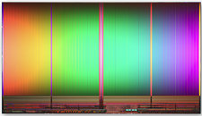
Manufactured by IM Flash Technologies (IMFT), Intel and Micron's NAND flash joint venture, the 25nm process produces 8 gigabytes (GB) of storage in a single NAND device, creating a high-capacity storage solution for today's tiny consumer gadgets. It measures just 167mm2 -- small enough to fit through the hole in the middle of a compact disc (CD), yet packs more than 10 times the data capacity of that CD (a standard CD holds 700 megabytes of data).
With a committed focus and investment in NAND research and development, Intel and Micron have doubled NAND density roughly every 18 months, which leads to smaller, more cost-efficient and higher capacity products. Intel and Micron formed IMFT in 2006, starting production with a 50nm process, followed by a 34nm process in 2008. With today's 25nm process, the companies are extending their process and fabrication leadership further with the introduction of the smallest semiconductor lithography available in the industry.
"To lead the entire semiconductor industry with the most advanced process technology is a phenomenal feat for Intel and Micron, and we look forward to further pushing the scaling limits," said Brian Shirley, vice president of Micron's memory group. "This production technology will enable significant benefits to our customers through higher density media solutions."
"Through our continued investment in IMFT, we're delivering leadership technology and manufacturing that enable the most cost-effective and reliable NAND memory," said Tom Rampone, vice president and general manager, Intel NAND Solutions Group. "This will help speed the adoption of solid-state drive solutions for computing."
The 25nm, 8GB device is sampling now and is expected to enter mass production in the second quarter of 2010. For consumer electronics manufacturers, the device provides the highest-density in a single 2 bits-per-cell multi-level cell (MLC) die that will fit an industry-standard, thin small-outline package (TSOP). Multiple 8GB devices can be stacked in a package to increase storage capacity. The new 25nm 8GB device reduces chip count by 50 percent compared to previous process generations, allowing for smaller, yet higher density designs and greater cost efficiencies. For example, a 256GB solid-state drive (SSD) can now be enabled with just 32 of these devices (versus 64 previously), a 32GB smartphone needs just four, and a 16GB flash card requires only two.
View at TechPowerUp Main Site
NAND flash memory stores data and other media contained in consumer electronics products, retaining information even when the power is turned off. The drive toward smaller NAND processes enables the continued development and introduction of new uses for the technology. Not only is the 25nm process the smallest NAND technology, it is also the smallest semiconductor technology in the world - a technological accomplishment that continues the advancement of more music, video, and other data in today's consumer electronics and computing applications.

Manufactured by IM Flash Technologies (IMFT), Intel and Micron's NAND flash joint venture, the 25nm process produces 8 gigabytes (GB) of storage in a single NAND device, creating a high-capacity storage solution for today's tiny consumer gadgets. It measures just 167mm2 -- small enough to fit through the hole in the middle of a compact disc (CD), yet packs more than 10 times the data capacity of that CD (a standard CD holds 700 megabytes of data).
With a committed focus and investment in NAND research and development, Intel and Micron have doubled NAND density roughly every 18 months, which leads to smaller, more cost-efficient and higher capacity products. Intel and Micron formed IMFT in 2006, starting production with a 50nm process, followed by a 34nm process in 2008. With today's 25nm process, the companies are extending their process and fabrication leadership further with the introduction of the smallest semiconductor lithography available in the industry.
"To lead the entire semiconductor industry with the most advanced process technology is a phenomenal feat for Intel and Micron, and we look forward to further pushing the scaling limits," said Brian Shirley, vice president of Micron's memory group. "This production technology will enable significant benefits to our customers through higher density media solutions."
"Through our continued investment in IMFT, we're delivering leadership technology and manufacturing that enable the most cost-effective and reliable NAND memory," said Tom Rampone, vice president and general manager, Intel NAND Solutions Group. "This will help speed the adoption of solid-state drive solutions for computing."
The 25nm, 8GB device is sampling now and is expected to enter mass production in the second quarter of 2010. For consumer electronics manufacturers, the device provides the highest-density in a single 2 bits-per-cell multi-level cell (MLC) die that will fit an industry-standard, thin small-outline package (TSOP). Multiple 8GB devices can be stacked in a package to increase storage capacity. The new 25nm 8GB device reduces chip count by 50 percent compared to previous process generations, allowing for smaller, yet higher density designs and greater cost efficiencies. For example, a 256GB solid-state drive (SSD) can now be enabled with just 32 of these devices (versus 64 previously), a 32GB smartphone needs just four, and a 16GB flash card requires only two.
View at TechPowerUp Main Site


 I do hope that you are right, but i think it will take at least half-year...
 i left myself open there