- Joined
- Oct 9, 2007
- Messages
- 47,233 (7.55/day)
- Location
- Hyderabad, India
| System Name | RBMK-1000 |
|---|---|
| Processor | AMD Ryzen 7 5700G |
| Motherboard | ASUS ROG Strix B450-E Gaming |
| Cooling | DeepCool Gammax L240 V2 |
| Memory | 2x 8GB G.Skill Sniper X |
| Video Card(s) | Palit GeForce RTX 2080 SUPER GameRock |
| Storage | Western Digital Black NVMe 512GB |
| Display(s) | BenQ 1440p 60 Hz 27-inch |
| Case | Corsair Carbide 100R |
| Audio Device(s) | ASUS SupremeFX S1220A |
| Power Supply | Cooler Master MWE Gold 650W |
| Mouse | ASUS ROG Strix Impact |
| Keyboard | Gamdias Hermes E2 |
| Software | Windows 11 Pro |
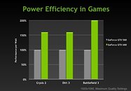
Despite the fact that NVIDIA is frantically seeking out other semiconductor foundries for high-volume manufacturing its 28 nm chip designs, and despite some looming irritants, NVIDIA appears to value its relationship with TSMC highly. NVIDIA's senior vice president for Advanced Technology Group Joe Greco, in a recent company blog post, credited close collaboration with TSMC for the stellar energy-efficiency (performance/Watt) figures NVIDIA's Kepler architecture has been able to achieve.
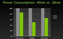
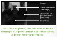
"The advancement that TSMC offered was a new optimized process technology. Kepler is manufactured using TSMC's 28nm high performance (HP) process, the foundry's most advanced 28nm process which uses their first-generation high-K metal gate (HKMG) technology and second generation SiGe (Silicon Germanium) straining," read the blog post. "Using TSMC's 28nm HP process enabled us to reduce active power by about 15 percent and leakage by about 50 percent compared to 40nm, resulting in an overall improvement in power efficiency of about 35 percent (see charts)."
Apart from advanced process technologies, NVIDIA credited professional collaboration with its long time foundry partner. According to Greco, groundwork for what led to today's Kepler chip began three years before tape-out, over the course of which the two companies set up a "Production Qualification Vehicle (PQV)" that allowed engineers from both sides to optimize the process. "Through repeated prototyping, we were able to optimize both the process and design, creating a more efficient Kepler design rather than simply a chip in a standard 28nm process," he writes. The entire blog post can be read here.
View at TechPowerUp Main Site
"The advancement that TSMC offered was a new optimized process technology. Kepler is manufactured using TSMC's 28nm high performance (HP) process, the foundry's most advanced 28nm process which uses their first-generation high-K metal gate (HKMG) technology and second generation SiGe (Silicon Germanium) straining," read the blog post. "Using TSMC's 28nm HP process enabled us to reduce active power by about 15 percent and leakage by about 50 percent compared to 40nm, resulting in an overall improvement in power efficiency of about 35 percent (see charts)."


Apart from advanced process technologies, NVIDIA credited professional collaboration with its long time foundry partner. According to Greco, groundwork for what led to today's Kepler chip began three years before tape-out, over the course of which the two companies set up a "Production Qualification Vehicle (PQV)" that allowed engineers from both sides to optimize the process. "Through repeated prototyping, we were able to optimize both the process and design, creating a more efficient Kepler design rather than simply a chip in a standard 28nm process," he writes. The entire blog post can be read here.
View at TechPowerUp Main Site


