- Joined
- Oct 9, 2007
- Messages
- 47,249 (7.54/day)
- Location
- Hyderabad, India
| System Name | RBMK-1000 |
|---|---|
| Processor | AMD Ryzen 7 5700G |
| Motherboard | ASUS ROG Strix B450-E Gaming |
| Cooling | DeepCool Gammax L240 V2 |
| Memory | 2x 8GB G.Skill Sniper X |
| Video Card(s) | Palit GeForce RTX 2080 SUPER GameRock |
| Storage | Western Digital Black NVMe 512GB |
| Display(s) | BenQ 1440p 60 Hz 27-inch |
| Case | Corsair Carbide 100R |
| Audio Device(s) | ASUS SupremeFX S1220A |
| Power Supply | Cooler Master MWE Gold 650W |
| Mouse | ASUS ROG Strix Impact |
| Keyboard | Gamdias Hermes E2 |
| Software | Windows 11 Pro |
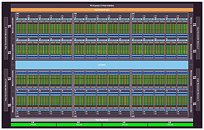
The upcoming "Pascal" GPU architecture from NVIDIA is shaping up to be a pixel-crunching monstrosity. Introduced as more of a number-cruncher in its Tesla P100 unveil at GTC 2016, we got our hands on the block diagram of the "GP100" silicon which drives it. To begin with, the GP100 is a multi-chip module, much like AMD's "Fiji," consisting of a large GPU die, four memory-stacks, and silicon wafer (interposer) acting as substrate for the GPU and memory stacks, letting NVIDIA drive microscopic wires between the two. The GP100 features a 4096-bit wide HBM2 memory interface, with typical memory bandwidths of up to 1 TB/s. On the P100, the memory ticks at 720 GB/s.
At its most top-level hierarchy, the GP100 is structured much like other NVIDIA GPUs, with the exception of two key interfaces - bus and memory. A PCI-Express gen 3.0 x16 host interface connects the GPU to your system, the GigaThread Engine distributes workload between six graphics processing clusters (GPCs). Eight memory controllers make up the 4096-bit wide HBM2 memory interface, and a new "High-speed Hub" component, wires out four NVLink ports. At this point it's not known if each port has a throughput of 80 GB/s (per-direction), or all four ports put together.


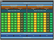
The GP100 features six graphics processing clusters (GPCs). These are highly independent subdivisions of the GPU, with their own render front and back-ends. With the "Pascal" architecture, at least with the way it's implemented on the GP100, each GPC features 10 streaming multiprocessors (SMs), the basic number crunching machinery of the GPU. Each SM holds 64 CUDA cores. The GPC hence holds a total of 640 CUDA cores, and the entire GP100 chip holds 3,840 CUDA cores. Other vital specs include 240 TMUs. On the Tesla P100, NVIDIA enabled just 56 of the 60 streaming multiprocessors, working out to a CUDA core count of 3,584.
The "Pascal" architecture appears to facilitate very high clock speeds. The Tesla P100, despite being an enterprise part, features a core clock speed as high as 1328 MHz, with GPU Boost frequency of 1480 MHz, and a TDP of 300W. This might scare you, but you have to take into account that the memory stacks have been moved to the GPU package, and so the heatsink interfacing with it all, will have to cope with the combined thermal loads of the GPU die, the memory stacks, and whatever else makes heat on the multi-chip module.
Lastly, there's the concept of NVLink. This interconnect developed in-house by NVIDIA makes multi-GPU setups work much like a modern multi-socket CPU machine, in which QPI (Intel) or HyperTransport (AMD) links provide super-highways between neighboring sockets. Each NVLink path offers a bandwidth of up to 80 GB/s (per direction), enabling true memory virtualization between multiple GPUs. This could prove useful for GPU-accelerated HPC systems, in which one GPU has to access memory controlled by a neighboring GPU, while the software sees the sum of the two GPUs' memory as one unified and contiguous block. The Pascal Unified Memory system lets advanced GPU programming models like CUDA 8 oversubscribe memory beyond what the GPU physically controls, and up to the system memory.
View at TechPowerUp Main Site
At its most top-level hierarchy, the GP100 is structured much like other NVIDIA GPUs, with the exception of two key interfaces - bus and memory. A PCI-Express gen 3.0 x16 host interface connects the GPU to your system, the GigaThread Engine distributes workload between six graphics processing clusters (GPCs). Eight memory controllers make up the 4096-bit wide HBM2 memory interface, and a new "High-speed Hub" component, wires out four NVLink ports. At this point it's not known if each port has a throughput of 80 GB/s (per-direction), or all four ports put together.


The GP100 features six graphics processing clusters (GPCs). These are highly independent subdivisions of the GPU, with their own render front and back-ends. With the "Pascal" architecture, at least with the way it's implemented on the GP100, each GPC features 10 streaming multiprocessors (SMs), the basic number crunching machinery of the GPU. Each SM holds 64 CUDA cores. The GPC hence holds a total of 640 CUDA cores, and the entire GP100 chip holds 3,840 CUDA cores. Other vital specs include 240 TMUs. On the Tesla P100, NVIDIA enabled just 56 of the 60 streaming multiprocessors, working out to a CUDA core count of 3,584.
The "Pascal" architecture appears to facilitate very high clock speeds. The Tesla P100, despite being an enterprise part, features a core clock speed as high as 1328 MHz, with GPU Boost frequency of 1480 MHz, and a TDP of 300W. This might scare you, but you have to take into account that the memory stacks have been moved to the GPU package, and so the heatsink interfacing with it all, will have to cope with the combined thermal loads of the GPU die, the memory stacks, and whatever else makes heat on the multi-chip module.
Lastly, there's the concept of NVLink. This interconnect developed in-house by NVIDIA makes multi-GPU setups work much like a modern multi-socket CPU machine, in which QPI (Intel) or HyperTransport (AMD) links provide super-highways between neighboring sockets. Each NVLink path offers a bandwidth of up to 80 GB/s (per direction), enabling true memory virtualization between multiple GPUs. This could prove useful for GPU-accelerated HPC systems, in which one GPU has to access memory controlled by a neighboring GPU, while the software sees the sum of the two GPUs' memory as one unified and contiguous block. The Pascal Unified Memory system lets advanced GPU programming models like CUDA 8 oversubscribe memory beyond what the GPU physically controls, and up to the system memory.
View at TechPowerUp Main Site


 Every year is like this. Summer = GP104; Winter = GP100.