• Welcome to TechPowerUp Forums, Guest! Please check out our forum guidelines for info related to our community.
  • The forums have been upgraded with support for dark mode. By default it will follow the setting on your system/browser. You may override it by scrolling to the end of the page and clicking the gears icon.

AMD Raja Koduri Confirms RX Vega Die Size at 484 mm²

Raevenlord

News Editor
Joined
Aug 12, 2016
Messages
3,755 (1.16/day)
Location
Portugal
System Name The Ryzening
Processor AMD Ryzen 9 5900X
Motherboard MSI X570 MAG TOMAHAWK
Cooling Lian Li Galahad 360mm AIO
Memory 32 GB G.Skill Trident Z F4-3733 (4x 8 GB)
Video Card(s) Gigabyte RTX 3070 Ti
Storage Boot: Transcend MTE220S 2TB, Kintson A2000 1TB, Seagate Firewolf Pro 14 TB
Display(s) Acer Nitro VG270UP (1440p 144 Hz IPS)
Case Lian Li O11DX Dynamic White
Audio Device(s) iFi Audio Zen DAC
Power Supply Seasonic Focus+ 750 W
Mouse Cooler Master Masterkeys Lite L
Keyboard Cooler Master Masterkeys Lite L
Software Windows 10 x64
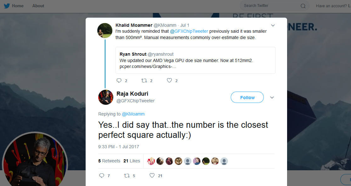
AMD's Raja Koduri, leader of the company's Radeon Technologies Group, has somewhat informally confirmed on Twitter the overall die size of AMD's Vega chips. After PC Perspective updated their prognosis regarding Vega's die-size to a beefier 512 mm², Twitter users plied Raja Koduri with questions regarding this subject. Koduri declined to answer directly, actually opting for a somewhat cryptic response, in that " (...) the answer [to Vega's die-size] is the closest perfect square number actually:)".

For the math-savvy around here (or even just for those of you who have read the headline), that particular equation should solve towards a perfect 484 mm² die area. Good news for AMD: this isn't the company's biggest die-size in consumer GPUs ever. That dubious honor goes to the company's Fiji XT silicon which powered the company's R9 Fury X, coming in at a staggering 596 mm² in the 28 nm process. For comparison, AMD's current Polaris 20 XTX-based RX 580 chip comes in at slightly less than half the confirmed RX Vega's die-size, at a much more yield-friendly 232 mm². NVIDIA's current top-of-the-line Titan Xp comes in at a slightly smaller 471 mm² die-size.


View at TechPowerUp Main Site
 
Die size is bigger cos include memory chip?
 
Die size is bigger cos include memory chip?

No, the memory is mounted on an interposer, it's not part of the die. That would waste too many chips and would make the chips prohibitively expensive.
 
Here is to hope that big die gets some good performance (gaming, neither mining nor "Prosumer use") later down the road.
 
This brings back (not so good) memories about 2900 xt, 420mm2


The only good thing about it was HD4xxx after
 
No, the memory is mounted on an interposer, it's not part of the die. That would waste too many chips and would make the chips prohibitively expensive.

He might be talking about the high bandwidth cache which would make for large die sizes.
 
I wonder if they could put two chips together working as one (not crossfire) using the Infinity Fabric, somewhat like they did with Threadripper, would that be feasible?
 
I wonder if they could put two chips together working as one (not crossfire) using the Infinity Fabric, somewhat like they did with Threadripper, would that be feasible?

Vega supports infinity fabric, however I think that is what they will be doing with Navi.
 
can some1 please explain me what means "Die Size"
 
Here is to hope that big die gets some good performance (gaming, neither mining nor "Prosumer use") later down the road.
We've seen an all-in-one card with older drivers (main improvement will be gaming), wx9100 will be for professional use only with certified drivers or something and rx vega will be for gaming only and its die is smaller than vega FE's die for no obvious reason. Maybe vega 10 has much lower latency or something because of the shorter distances between its components or something. Interesting to see the wx9100 and a "small", yet conplete vega 10.
 
can some1 please explain me what means "Die Size"
The die is one of the many silicon squares that they cut out of the wafer during production.
 
so basicly if number lower its better?

The die is one of the many silicon squares that they cut out of the wafer during production.
 
But smaller with the same amount of streamprocessors is generally better.
That would require a smaller process node that is why I stated "within a gpu generation".
 
That would require a smaller process node that is why I stated "within a gpu generation".
Not necessarily. Optimizations can make almost as much difference as a smaller proces node sometimes if older versions were barely optimized.
 
Not necessarily. Optimizations can make almost as much difference as a smaller proces node sometimes if older versions were barely optimized.

Sure, that is true, but different uarch, would not qualify as the same GPU generation in my book.
 
So bigger than latest titan although nowhere as fast and quite a bit more power hungry.

Wake me up when Navi is there, as Vega woes are somehow not Raja's fault.
 
So bigger than latest titan although nowhere as fast and quite a bit more power hungry.

Wake me up when Navi is there, as Vega woes are somehow not Raja's fault.
Titans are like bad geforce cards with bigger dies. At least vega FE has some workstation optimizations. Only useful for the budget pro or rich arabian oil guy's son that wants everything computer related, but that's why there will also be rx vega and the wx 9100 for gamers and professionals with a decent budget respectively. Rich arabian oil guy's son will buy those as well, because why not?!
 
This brings back (not so good) memories about 2900 xt, 420mm2


The only good thing about it was HD4xxx after

Actually, AMD followed up the vacuum-loud 2900XT with the highly successful 38x0 series. The 3870 was one of my favorite cards, as it could easily run Bioshock with DX10 goodness, and it matched up with the 8800 GT quite well.
 
so basicly if number lower its better?
For die size, if you're talking about compute power, a bigger die will give you more computing power always, unless cavemen designed the die.
If all things are equal--same transistor/trace size inside the die (same manufacturing process) then bigger is always better.... The bigger the die, the more transistors you can cram into it, therefore, the more you can process in one cycle.
When they shrink down to a new process, say from 24nm to 14nm, the die shrinks to about half it's original size and keeps the same amount of transistors inside. Both chips can process the same amount of information in one cycle, just that the 14nm process die will do it with less power consumption.
There's die size and process size. Normally when they shrink down to a new process, they will just add more transistors to make up for the freed up power consumption.
For apples to apples comparison, a smaller die and process version of the same chip will be a 'better' chip.
So, yes, a smaller die is better. And no, a smaller die is not better.
 
Last edited:
I wonder if they could put two chips together working as one (not crossfire) using the Infinity Fabric, somewhat like they did with Threadripper, would that be feasible?

That's probably what Navi will look like.

And it is the path forward for almost everything. Nvidia has NVLink, Intel has Quickpath, etc.
 
Back
Top