- Joined
- Oct 9, 2007
- Messages
- 47,296 (7.53/day)
- Location
- Hyderabad, India
| System Name | RBMK-1000 |
|---|---|
| Processor | AMD Ryzen 7 5700G |
| Motherboard | ASUS ROG Strix B450-E Gaming |
| Cooling | DeepCool Gammax L240 V2 |
| Memory | 2x 8GB G.Skill Sniper X |
| Video Card(s) | Palit GeForce RTX 2080 SUPER GameRock |
| Storage | Western Digital Black NVMe 512GB |
| Display(s) | BenQ 1440p 60 Hz 27-inch |
| Case | Corsair Carbide 100R |
| Audio Device(s) | ASUS SupremeFX S1220A |
| Power Supply | Cooler Master MWE Gold 650W |
| Mouse | ASUS ROG Strix Impact |
| Keyboard | Gamdias Hermes E2 |
| Software | Windows 11 Pro |
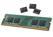
Samsung Electronics Co., Ltd., the world leader in advanced memory technology, announced today that it has begun mass producing the industry's first 2nd-generation of 10-nanometer class (1y-nm), 8-gigabit (Gb) DDR4 DRAM. For use in a wide range of next-generation computing systems, the new 8 Gb DDR4 features the highest performance and energy efficiency for an 8 Gb DRAM chip, as well as the smallest dimensions.
"By developing innovative technologies in DRAM circuit design and process, we have broken through what has been a major barrier for DRAM scalability," said Gyoyoung Jin, president of Memory Business at Samsung Electronics. "Through a rapid ramp-up of the 2nd-generation 10 nm-class DRAM, we will expand our overall 10 nm-class DRAM production more aggressively, in order to accommodate strong market demand and continue to strengthen our business competitiveness."

Samsung's 2nd-generation 10nm-class 8 Gb DDR4 features an approximate 30 percent productivity gain over the company's 1st-generation 10 nm-class 8 Gb DDR4. In addition, the new 8 Gb DDR4's performance levels and energy efficiency have been improved about 10 and 15 percent respectively, thanks to the use of an advanced, proprietary circuit design technology. The new 8Gb DDR4 can operate at 3,600 megabits per second (Mbps) per pin, compared to 3,200 Mbps of the company's 1x-nm 8 Gb DDR4.
To enable these achievements, Samsung has applied new technologies, without the use of an EUV process. The innovation here includes use of a high-sensitivity cell data sensing system and a progressive "air spacer" scheme.
In the cells of Samsung's 2nd-generation 10 nm-class DRAM, a newly devised data sensing system enables a more accurate determination of the data stored in each cell, which leads to a significant increase in the level of circuit integration and manufacturing productivity.
The new 10 nm-class DRAM also makes use of a unique air spacer that has been placed around its bit lines to dramatically decrease parasitic capacitance. Use of the air spacer enables not only a higher level of scaling, but also rapid cell operation.
With these advancements, Samsung is now accelerating its plans for much faster introductions of next-generation DRAM chips and systems, including DDR5, HBM3, LPDDR5 and GDDR6, for use in enterprise servers, mobile devices, supercomputers, HPC systems and high-speed graphics cards.
Samsung has finished validating its 2nd-generation 10 nm-class DDR4 modules with CPU manufacturers, and next plans to work closely with its global IT customers in the development of more efficient next-generation computing systems.
In addition, the world's leading DRAM producer expects to not only rapidly increase the production volume of the 2nd-generation 10nm-class DRAM lineups, but also to manufacture more of its mainstream 1st-generation 10 nm-class DRAM, which together will meet the growing demands for DRAM in premium electronic systems worldwide.
View at TechPowerUp Main Site
"By developing innovative technologies in DRAM circuit design and process, we have broken through what has been a major barrier for DRAM scalability," said Gyoyoung Jin, president of Memory Business at Samsung Electronics. "Through a rapid ramp-up of the 2nd-generation 10 nm-class DRAM, we will expand our overall 10 nm-class DRAM production more aggressively, in order to accommodate strong market demand and continue to strengthen our business competitiveness."

Samsung's 2nd-generation 10nm-class 8 Gb DDR4 features an approximate 30 percent productivity gain over the company's 1st-generation 10 nm-class 8 Gb DDR4. In addition, the new 8 Gb DDR4's performance levels and energy efficiency have been improved about 10 and 15 percent respectively, thanks to the use of an advanced, proprietary circuit design technology. The new 8Gb DDR4 can operate at 3,600 megabits per second (Mbps) per pin, compared to 3,200 Mbps of the company's 1x-nm 8 Gb DDR4.
To enable these achievements, Samsung has applied new technologies, without the use of an EUV process. The innovation here includes use of a high-sensitivity cell data sensing system and a progressive "air spacer" scheme.
In the cells of Samsung's 2nd-generation 10 nm-class DRAM, a newly devised data sensing system enables a more accurate determination of the data stored in each cell, which leads to a significant increase in the level of circuit integration and manufacturing productivity.
The new 10 nm-class DRAM also makes use of a unique air spacer that has been placed around its bit lines to dramatically decrease parasitic capacitance. Use of the air spacer enables not only a higher level of scaling, but also rapid cell operation.
With these advancements, Samsung is now accelerating its plans for much faster introductions of next-generation DRAM chips and systems, including DDR5, HBM3, LPDDR5 and GDDR6, for use in enterprise servers, mobile devices, supercomputers, HPC systems and high-speed graphics cards.
Samsung has finished validating its 2nd-generation 10 nm-class DDR4 modules with CPU manufacturers, and next plans to work closely with its global IT customers in the development of more efficient next-generation computing systems.
In addition, the world's leading DRAM producer expects to not only rapidly increase the production volume of the 2nd-generation 10nm-class DRAM lineups, but also to manufacture more of its mainstream 1st-generation 10 nm-class DRAM, which together will meet the growing demands for DRAM in premium electronic systems worldwide.
View at TechPowerUp Main Site


