• Welcome to TechPowerUp Forums, Guest! Please check out our forum guidelines for info related to our community.

NVIDIA GeForce GTX 1180 Bare PCB Pictured

btarunr

Editor & Senior Moderator
Staff member
Joined
Oct 9, 2007
Messages
47,878 (7.38/day)
Location
Dublin, Ireland
System Name RBMK-1000
Processor AMD Ryzen 7 5700G
Motherboard Gigabyte B550 AORUS Elite V2
Cooling DeepCool Gammax L240 V2
Memory 2x 16GB DDR4-3200
Video Card(s) Galax RTX 4070 Ti EX
Storage Samsung 990 1TB
Display(s) BenQ 1440p 60 Hz 27-inch
Case Corsair Carbide 100R
Audio Device(s) ASUS SupremeFX S1220A
Power Supply Cooler Master MWE Gold 650W
Mouse ASUS ROG Strix Impact
Keyboard Gamdias Hermes E2
Software Windows 11 Pro
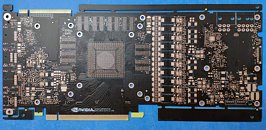
Here are some of the first pictures of the bare printed circuit board (PCB) of NVIDIA's upcoming GeForce GTX 1180 graphics card (dubbed PG180), referred to by the person who originally posted them as "GTX 2080" (it seems the jury is still out on the nomenclature). The PCB looks hot from the press, with its SMT points and vias still exposed. The GT104 GPU traces hint at a package that's about the size of a GP104 or its precessors. It's wired to eight memory chips on three sides, confirming a 256-bit wide memory bus. Display outputs appear flexible, for either 2x DisplayPort + 2x HDMI, or 3x DisplayPort + 1x HDMI configurations.

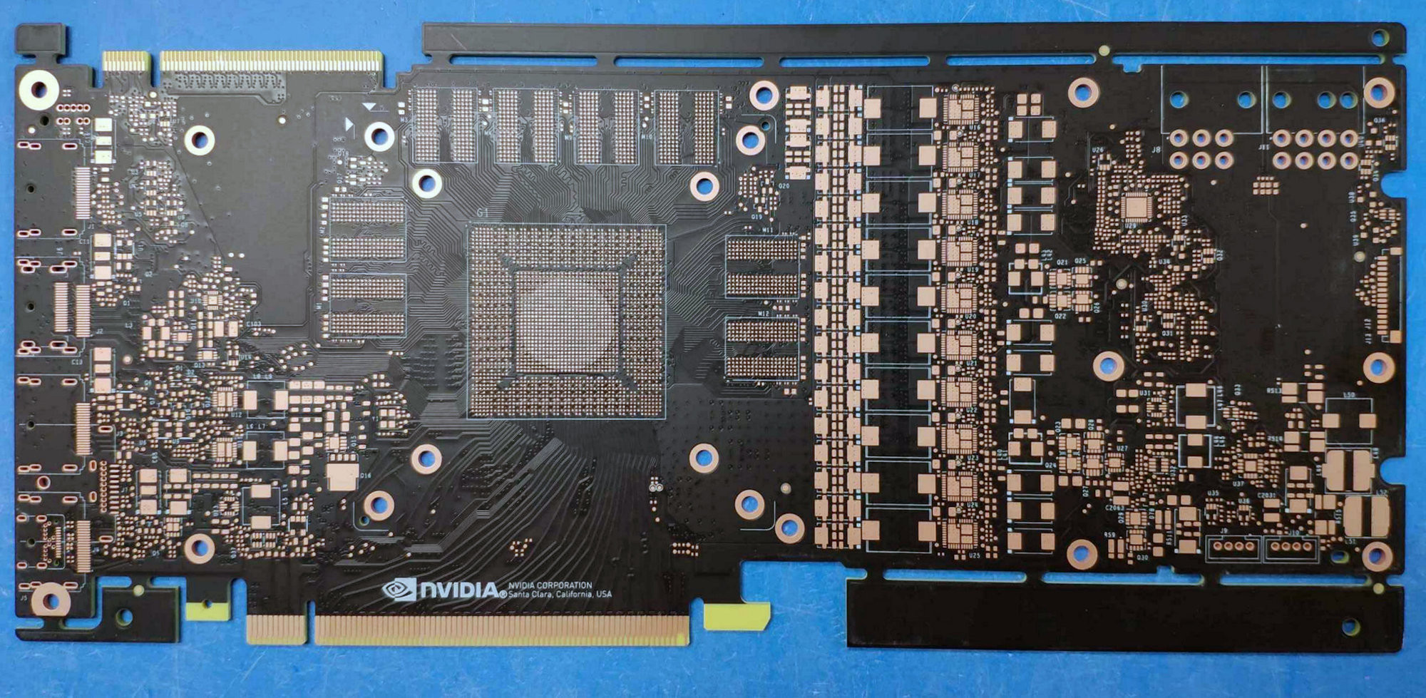
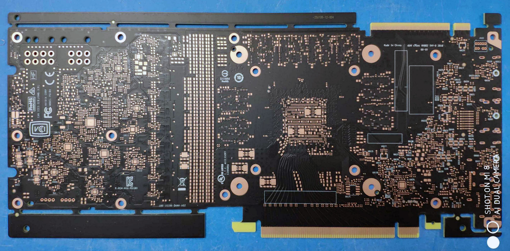
The VRM setup is surprisingly powerful for a card that's supposed to succeed the ~180W GeForce GTX 1080, which can make do with a single 8-pin PCIe power input. The card draws power from a combination of 6-pin and 8-pin PCIe power connectors. There is a purportedly 10-phase VCore side, which in all likelihood is a 5-phase setup with "dumb" phase-doubling; and similarly, a 2-phase memory power (which could again be doubled single-phase). The SLI-HB fingers also make way. There's a new connector that looks like a single SLI finger and an NVLink finger arranged side-by-side. NVIDIA still hasn't given up on multi-GPU. NVLink is a very broad interconnect, in terms of bandwidth. NVIDIA probably needs that for multi-GPU setups to work with not just high resolutions (4K, 5K, or even 8K), but also higher bit-depth, higher refresh-rates, HDR, and other exotic data. The reverse side doesn't have much action other than traces for the VRM controllers, phase doublers, and an unusually large bank of SMT capacitors (the kind seen on AMD PCBs with MCM GPUs).


View at TechPowerUp Main Site
 
I wonder what are the chances that NVIDIA will decide to opt for 12GB config instead of 8GB.
I'm a little afraid that this will cannibalize pro cards for deep learning purposes.

About the phases - I don't see why this cant be a full blown 8+2 design. Its not uncommon. They could also just not solder the extra unusable phases to the controller, much like how its done on 1080:

nvidia-geforce-gtx-1080-internal-Front_PCB.png
 
  • Like
Reactions: ppn
so likely the vrm is using a 5+1 setup with doublers, i expect it to be around 30 watts less than a 1080ti due to the smaller memory bus and 12nm, if most of the volta improvements trickle down this should be great in d3d12 as GV100 has a hardware scheduler, unlike all uArchs since fermi i believe (correct me if im wrong). its also interesting to see that GDDR6 seems to be physically larger than the GDDR5X used on the 1080
 
  • Like
Reactions: ppn
where have you seen 12gb in production on what manufacturer website
die estimation 360?

officially gddr6 measures 14x12 mm, 5x 14x10.
 
where have you seen 12gb in production on what manufacturer website

GDDR6 is also available in 12Gb chips, so one assume that to keep safe space from pro-sumer solutions, but still provide more than last gen, 12GB of video memory might be optimal.
 
Given GTX 1080Ti has 11GB, it would be weird to release its successor with WAY less. 11GB was weird number by itself. Odd numbers are rare and are very weird. 3GB HD7900 cards, 5GB GTX 1050Ti's, 11GB GTX 1080Ti, 3,5GB GTX 970 ;) etc These are very rare actually.
 
Well soon will be seeing filled up version..
 
wider bus could mean as much as 16gb of memory
 
Hm, could be a Quadro/Telsa PCB because of the NVLink and beefy VRMs but also a Geforce with those solder pads for VirtualLink.
 
wider bus could mean as much as 16gb of memory

Or narrower...

Let me just add, I don't think the card above is a GTX 2080. The specs don't really add up. I think it's a Quadro of sorts.
 
not in production. in sampling. it could have piggy backed 16x1GB but at the price of 25$ per GB not worth it.

As of January this year Samsung confirmed it's in production. It may not be in GA for consumer products but I would not be surprised if Nvidia's next-gen flagship is the first.
 
Sk Hynix and Micron have also confirmed volume production of GDDR6.

Looking at that PCB you can see those memory placements are indeed BGA-180 packages, so yeah definitely GDDR6.
 
I See Two Fan headers, so maybe this is not a founders edition. I doubt Nvidia changed to a 2 fan cooler.
 
Sk Hynix and Micron have also confirmed volume production of GDDR6.

Looking at that PCB you can see those memory placements are indeed BGA-180 packages, so yeah definitely GDDR6.

I don't think there was ever any doubt that this board used GDDR6. But the supply of 16Gbit packages is iffy, so it's possible that the first cards will be 8GB only.
 
Huh.. Figures the EEC went over some manli cards with the gpu name GA104. Seems Ampere... Also seems GTX 20 series
 
Power consumption at least 200W and closer to 250W more possible. Only way to have a bit higher than 1080Ti power at 12nm. So, 1170 between 1080 and 1080Ti and 1160 close to 1070. My 5 cents.
 
Or narrower...

Let me just add, I don't think the card above is a GTX 2080. The specs don't really add up. I think it's a Quadro of sorts.

Same and the traces are so beefy, power delivery seems to an issue they have in mind.
 
It has model PG180 written on it twice and 180 appears in the model extended model number.


GTX 1080 has PCB number 180-1G413-DAAA-A00 where this PCB is 180-1G180-DAAA-A02. Looks like an iteration on the previous design.
 
The board appears to have a layout that can accommodate four DP ports as the default configuration.
One DP port can be replaced by an HDMI port. (second from top)
One DP port can be replaced by what appears to be a USB-C port. (lowest one)
Finally the bottom tow DP ports seems to be replaceable by a port I don't recognise, that's set further back on the PCB. It's possible it's a D-Sub connector, but that would surely be madness, no?
 
With DRAM shortage and brand new GDDR6 combined, it's gonna be one expensive card. I have no doubt it will be priced higher than 1080 until AMD release something to counter it
 
Given GTX 1080Ti has 11GB, it would be weird to release its successor with WAY less. 11GB was weird number by itself. Odd numbers are rare and are very weird. 3GB HD7900 cards, 5GB GTX 1050Ti's, 11GB GTX 1080Ti, 3,5GB GTX 970 ;) etc These are very rare actually.

Odd VRAM numbers are not rare by any stretch. It's all down to available bus. Here's a few past examples of GPUs that had 'weird' VRAM arrangements.

8800 GTS - 320-bit - 320/640MB (cut-down from 384-bit)
8800 GTX - 384-bit - 768MB
GTX 260/275 - 448-bit - 896/1792MB (cut down from 512-bit)
GTX 460/460 v2 - 192-bit - 768/1536MB (cut down from 256-bit)
GTX 480/580 - 384-bit - 1536/3072MB
GTX 470/570 - 320-bit - 1280MB (cut down from 384-bit)
GT 545 - 192-bit - 1536/3072MB

Quadro FX 5600 - 384-bit - 1536MB
Quadro 6000 - 384-bit - 6144MB

Nothing new to nVidia. They've been doing this for over a decade, and will continue to.

GTX 1080 has PCB number 180-1G413-DAAA-A00 where this PCB is 180-1G180-DAAA-A02. Looks like an iteration on the previous design.

DAAA is nVidia's test pattern notation. 180 is their PCB signature, and 1GXXX is where the real info is. So 1G180 (PG180) is what tells us this is a completely new design, DAAA tells us it's a test pattern, and A02 just says it's the second test pattern for PG180. Compare this PCB to a reference GTX 1080 and the similarities are scarce.

Test pattern notation does not necessarily get removed from a final revision card, just for clarification. The revision number will generally change if anything is modified. This card is in a secondary stage of modification, but it could remain the final version.

Edit: I've been corrected. DAAA is not an indication of test patterns, it appears to be a generational notation starting with Pascal. (occupying what previously was the 11xx marking). My confusion stems from the appearance of DAXXXXXX stickers on many qualification and engineering boards, and I attributed that to the new markings. They are not related.
 
Last edited:
The board appears to have a layout that can accommodate four DP ports as the default configuration.
One DP port can be replaced by an HDMI port. (second from top)
One DP port can be replaced by what appears to be a USB-C port. (lowest one)
Finally the bottom tow DP ports seems to be replaceable by a port I don't recognise, that's set further back on the PCB. It's possible it's a D-Sub connector, but that would surely be madness, no?
Top to bottom:
DisplayPort
DisplayPort or HDMI
DisplayPort
DisplayPort or USB3-C (Thunderbolt 3?)
optional DVI-D single link
 
Last edited:
Back
Top