- Joined
- Aug 19, 2017
- Messages
- 2,662 (0.99/day)
What's New: This week at SEMICON West in San Francisco, Intel engineering leaders provided an update on Intel's advanced packaging capabilities and unveiled new building blocks, including innovative uses of EMIB and Foveros together and a new Omni-Directional Interconnect (ODI) technology. When combined with Intel's world-class process technologies, new packaging capabilities will unlock customer innovations and deliver the computing systems of tomorrow.
"Our vision is to develop leadership technology to connect chips and chiplets in a package to match the functionality of a monolithic system-on-chip. A heterogeneous approach gives our chip architects unprecedented flexibility to mix and match IP blocks and process technologies with various memory and I/O elements in new device form factors. Intel's vertically integrated structure provides an advantage in the era of heterogeneous integration, giving us an unmatched ability to co-optimize architecture, process and packaging to deliver leadership products." -Babak Sabi, Intel corporate vice president, Assembly and Test Technology Development.

Why It's Important: Chip packaging has always played a critical - if under-recognized - role in the electronics supply chain. As the physical interface between the processor and the motherboard, the package provides a landing zone for a chip's electrical signals and power supply. As the electronics industry transitions to the data-centric era, advanced packaging will play a much larger role than it has in the past.
More than just the final step in the manufacturing process, packaging is becoming a catalyst for product innovation. Advanced packaging techniques allow integration of diverse computing engines across multiple process technologies with performance parameters similar to a single die, but with a platform scope that far exceeds the die-size limit of single-die integration. These technologies will improve product-level performance, power and area while enabling a complete rethinking of system architecture.
What are Intel's Updates: Intel is a leader in advanced packaging technology, with current offerings spanning both 2D and 3D approaches. At SEMICON West, Intel unveiled three new technologies that will open a new dimension in product architecture:
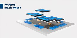
Co-EMIB: Intel's EMIB and Foveros technologies leverage high-density interconnects to enable high bandwidth at low power, with I/O density on par with or better than competitive approaches. The company's new Co-EMIB technology enables the linkage of even more computing performance and capability together. Co-EMIB allows for the interconnection of two or more Foveros elements with essentially the performance of a single chip. And designers can also connect analog, memory and other tiles with very high bandwidth and at very low power.
ODI: Intel's new Omni-Directional Interconnect provides even greater flexibility for communication among chiplets in a package. The top chip can communicate horizontally with other chiplets, similar to EMIB. It can also communicate vertically with through-silicon vias (TSVs) in the base die below, similar to Foveros. And ODI leverages large vertical vias to allow power delivery to the top die directly from the package substrate. Much larger than traditional TSVs, the large vias have lower resistance, providing more robust power delivery simultaneously with higher bandwidth and lower latency enabled through stacking. At the same time, this approach reduces the number of TSVs required in the base die, freeing up more area for active transistors and optimizing die size.
MDIO: Building upon its Advanced Interface Bus (AIB) PHY level interconnect, Intel disclosed a new die-to-die interface called MDIO. The technology enables a modular approach to system design with a library of chiplet intellectual property blocks. MDIO provides better power efficiency and more than double the pin speed and bandwidth density offered by AIB.
Collectively, these technologies are complementary tools in a powerful toolbox. When combined with Intel's process technologies, they form the underlying color palette for the creativity of its chip architects - giving them the freedom to dream up new products.

View at TechPowerUp Main Site
"Our vision is to develop leadership technology to connect chips and chiplets in a package to match the functionality of a monolithic system-on-chip. A heterogeneous approach gives our chip architects unprecedented flexibility to mix and match IP blocks and process technologies with various memory and I/O elements in new device form factors. Intel's vertically integrated structure provides an advantage in the era of heterogeneous integration, giving us an unmatched ability to co-optimize architecture, process and packaging to deliver leadership products." -Babak Sabi, Intel corporate vice president, Assembly and Test Technology Development.

Why It's Important: Chip packaging has always played a critical - if under-recognized - role in the electronics supply chain. As the physical interface between the processor and the motherboard, the package provides a landing zone for a chip's electrical signals and power supply. As the electronics industry transitions to the data-centric era, advanced packaging will play a much larger role than it has in the past.
More than just the final step in the manufacturing process, packaging is becoming a catalyst for product innovation. Advanced packaging techniques allow integration of diverse computing engines across multiple process technologies with performance parameters similar to a single die, but with a platform scope that far exceeds the die-size limit of single-die integration. These technologies will improve product-level performance, power and area while enabling a complete rethinking of system architecture.
What are Intel's Updates: Intel is a leader in advanced packaging technology, with current offerings spanning both 2D and 3D approaches. At SEMICON West, Intel unveiled three new technologies that will open a new dimension in product architecture:
Co-EMIB: Intel's EMIB and Foveros technologies leverage high-density interconnects to enable high bandwidth at low power, with I/O density on par with or better than competitive approaches. The company's new Co-EMIB technology enables the linkage of even more computing performance and capability together. Co-EMIB allows for the interconnection of two or more Foveros elements with essentially the performance of a single chip. And designers can also connect analog, memory and other tiles with very high bandwidth and at very low power.
ODI: Intel's new Omni-Directional Interconnect provides even greater flexibility for communication among chiplets in a package. The top chip can communicate horizontally with other chiplets, similar to EMIB. It can also communicate vertically with through-silicon vias (TSVs) in the base die below, similar to Foveros. And ODI leverages large vertical vias to allow power delivery to the top die directly from the package substrate. Much larger than traditional TSVs, the large vias have lower resistance, providing more robust power delivery simultaneously with higher bandwidth and lower latency enabled through stacking. At the same time, this approach reduces the number of TSVs required in the base die, freeing up more area for active transistors and optimizing die size.
MDIO: Building upon its Advanced Interface Bus (AIB) PHY level interconnect, Intel disclosed a new die-to-die interface called MDIO. The technology enables a modular approach to system design with a library of chiplet intellectual property blocks. MDIO provides better power efficiency and more than double the pin speed and bandwidth density offered by AIB.
Collectively, these technologies are complementary tools in a powerful toolbox. When combined with Intel's process technologies, they form the underlying color palette for the creativity of its chip architects - giving them the freedom to dream up new products.

View at TechPowerUp Main Site


