- Joined
- Aug 19, 2017
- Messages
- 2,679 (0.99/day)
During its GPU Technology Conference (GTC) in China, Mr. Bill Dally—NVIDIA's chief scientist and SVP of research—has presented many interesting things about how the company plans to push the future of HPC, AI, graphics, healthcare, and edge computing. Mr. Dally has presented NVIDIA's research efforts and what is the future vision for its products. Among one of the most interesting things presented was a plan to ditch the standard electrical data transfer and use the speed of light to scale and advance node communication. The new technology utilizing optical data transfer is supposed to bring the power required to transfer by a significant amount.
The proposed plan by the company is to use an optical NVLink equivalent. While the current NVLink 2.0 chip uses eight pico Joules per bit (8 pJ/b) and can send signals only to 0.3 meters without any repeaters, the optical replacement is capable of sending data anywhere from 20 to 100 meters while consuming half the power (4 pJ/b). NVIDIA has conceptualized a system with four GPUs in a tray, all of which are connected by light. To power such a setup, there are lasers that produce 8-10 wavelengths. These wavelengths are modulated onto this at a speed of 25 Gbit/s per wavelength, using ring resonators. On the receiving side, ring photodetectors are used to pick up the wavelength and send it to the photodetector. This technique ensures fast data transfer capable of long distances.

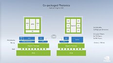
And that is not even all of it. To integrate everything, NVIDIA needs to combine it with chip packaging technology. Pictured below is a setup where the GPU and memory combination sits on a silicon interposer, which itself is placed on top of an organic package. This organic package is connected to the photonic integrated circuit (PIC). Further, there is an electrical interface chip (EIC) that converts the electrical signals coming from the GPU, using resonators, to optical signals. Optical interconnect needs a similarly built switch on its side.

Using these techniques, NVIDIA says that in the future there could be systems with 1000s of interconnected GPUs, each of which talks to another using a speed of light. It is only a matter of time before the technology reaches the market, however, there are no guarantees as this is only a research project for now.

View at TechPowerUp Main Site
The proposed plan by the company is to use an optical NVLink equivalent. While the current NVLink 2.0 chip uses eight pico Joules per bit (8 pJ/b) and can send signals only to 0.3 meters without any repeaters, the optical replacement is capable of sending data anywhere from 20 to 100 meters while consuming half the power (4 pJ/b). NVIDIA has conceptualized a system with four GPUs in a tray, all of which are connected by light. To power such a setup, there are lasers that produce 8-10 wavelengths. These wavelengths are modulated onto this at a speed of 25 Gbit/s per wavelength, using ring resonators. On the receiving side, ring photodetectors are used to pick up the wavelength and send it to the photodetector. This technique ensures fast data transfer capable of long distances.

And that is not even all of it. To integrate everything, NVIDIA needs to combine it with chip packaging technology. Pictured below is a setup where the GPU and memory combination sits on a silicon interposer, which itself is placed on top of an organic package. This organic package is connected to the photonic integrated circuit (PIC). Further, there is an electrical interface chip (EIC) that converts the electrical signals coming from the GPU, using resonators, to optical signals. Optical interconnect needs a similarly built switch on its side.


Using these techniques, NVIDIA says that in the future there could be systems with 1000s of interconnected GPUs, each of which talks to another using a speed of light. It is only a matter of time before the technology reaches the market, however, there are no guarantees as this is only a research project for now.

View at TechPowerUp Main Site


 . So does this eventually lead to consumer cards with some kinda special ability to connect to each other to boost performance... wouldn't that be interesting? Wonder what it might be called?