Raevenlord
News Editor
- Joined
- Aug 12, 2016
- Messages
- 3,755 (1.20/day)
- Location
- Portugal
| System Name | The Ryzening |
|---|---|
| Processor | AMD Ryzen 9 5900X |
| Motherboard | MSI X570 MAG TOMAHAWK |
| Cooling | Lian Li Galahad 360mm AIO |
| Memory | 32 GB G.Skill Trident Z F4-3733 (4x 8 GB) |
| Video Card(s) | Gigabyte RTX 3070 Ti |
| Storage | Boot: Transcend MTE220S 2TB, Kintson A2000 1TB, Seagate Firewolf Pro 14 TB |
| Display(s) | Acer Nitro VG270UP (1440p 144 Hz IPS) |
| Case | Lian Li O11DX Dynamic White |
| Audio Device(s) | iFi Audio Zen DAC |
| Power Supply | Seasonic Focus+ 750 W |
| Mouse | Cooler Master Masterkeys Lite L |
| Keyboard | Cooler Master Masterkeys Lite L |
| Software | Windows 10 x64 |
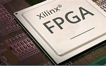
AMD has applied for a United States Patent that describes a CPU design with FPGA (Field-Programmable Gate Array) elements integrated into its core design. Titled "Method and Apparatus for Efficient Programmable Instructions in Computer Systems", the patent application describes a CPU with FPGA elements inscribed into its very core design, where the FPGA elements actually share CPU resources such as registers for floating-point and integer execution units. This patent undoubtedly comes in the wake of AMD's announced Xilinx acquisition plans, and brings FPGA and CPU marriages to a whole other level. FPGA,as the name implies, are hardware constructions which can reconfigure themselves according to predetermined tables (which can also be updated) to execute desired and specific functions.
Intel have themselves already shipped a CPU + FPGA combo in the same package; the company's Xeon 6138P, for example, includes an Arria 10 GX 1150 FPGA on-package, offering 1,150,000 logic elements. However, this is simply a CPU + FPGA combo on the same substrate; not a native, core-integrated FPGA design. Intel's product has severe performance and latency penalties due to the fact that complex operations performed in the FPGA have to be brought out of the CPU, processed in the FPGA, and then its results have to be returned to the CPU. AMD's design effectively ditches that particular roundabout, and should thus allow for much higher performance.


Some of the more interesting claims in the patent application are listed below:
As it stands, this sort of design would allow, in theory, for an updatable CPU that might never need to be upgraded when it comes to new instruction support: since FPGA is a programmable hardware logic, a simple firmware update could allow the CPU to reconfigure its FPGA array so as to be able to process new, exotic instructions as they are released. Another argument for this integration is that in this way, some fixed-function silicon that is today found in CPUs and that serve to support legacy x86 instructions could be left out of the die, to be taken care of by the FPGA package itself - enabling a still-on-board hardware accelerator for when (and if) these instructions are required.
This would also allow AMD to trim the CPU of the "dark silicon" that is currently present - essentially, highly specialized hardware acceleration blocks that sit idly, as a waste of die space, when not in use. The bottom line is this: CPUs with lower die space reserved for highly specialized operations, thus with more die area available for other resources (such as more cores), and with integrated, per-core FPGA elements that would on-the-fly reconfigure themselves according to processing needs. And if there are no exotic operations required (such as AI inferencing and acceleration, AVX (for example), video hardware acceleration, or other workloads, then the FPGA elements can just be reconfigured to "turbo" the CPU's own floating point and integer units, increasing available resources. An interesting patent application, for sure.
View at TechPowerUp Main Site
Intel have themselves already shipped a CPU + FPGA combo in the same package; the company's Xeon 6138P, for example, includes an Arria 10 GX 1150 FPGA on-package, offering 1,150,000 logic elements. However, this is simply a CPU + FPGA combo on the same substrate; not a native, core-integrated FPGA design. Intel's product has severe performance and latency penalties due to the fact that complex operations performed in the FPGA have to be brought out of the CPU, processed in the FPGA, and then its results have to be returned to the CPU. AMD's design effectively ditches that particular roundabout, and should thus allow for much higher performance.


Some of the more interesting claims in the patent application are listed below:
- Processor includes one or more reprogrammable execution units which can be programmed to execute different types of customized instructions
- When a processor loads a program, it also loads a bitfile associated with the program which programs the PEU to execute the customized instruction
- Decode and dispatch unit of the CPU automatically dispatches the specialized instructions to the proper PEUs
- PEU shares registers with the FP and Int EUs.
- PEU can accelerate Int or FP workloads as well if speedup is desired
- PEU can be virtualized while still using system security features
- Each PEU can be programmed differently from other PEUs in the system
- PEUs can operate on data formats that are not typical FP32/FP64 (e.g. Bfloat16, FP16, Sparse FP16, whatever else they want to come up with) to accelerate machine learning, without needing to wait for new silicon to be made to process those data types.
- PEUs can be reprogrammed on-the-fly (during runtime)
- PEUs can be tuned to maximize performance based on the workload
- PEUs can massively increase IPC by doing more complex work in a single cycle
As it stands, this sort of design would allow, in theory, for an updatable CPU that might never need to be upgraded when it comes to new instruction support: since FPGA is a programmable hardware logic, a simple firmware update could allow the CPU to reconfigure its FPGA array so as to be able to process new, exotic instructions as they are released. Another argument for this integration is that in this way, some fixed-function silicon that is today found in CPUs and that serve to support legacy x86 instructions could be left out of the die, to be taken care of by the FPGA package itself - enabling a still-on-board hardware accelerator for when (and if) these instructions are required.
This would also allow AMD to trim the CPU of the "dark silicon" that is currently present - essentially, highly specialized hardware acceleration blocks that sit idly, as a waste of die space, when not in use. The bottom line is this: CPUs with lower die space reserved for highly specialized operations, thus with more die area available for other resources (such as more cores), and with integrated, per-core FPGA elements that would on-the-fly reconfigure themselves according to processing needs. And if there are no exotic operations required (such as AI inferencing and acceleration, AVX (for example), video hardware acceleration, or other workloads, then the FPGA elements can just be reconfigured to "turbo" the CPU's own floating point and integer units, increasing available resources. An interesting patent application, for sure.
View at TechPowerUp Main Site


