• Welcome to TechPowerUp Forums, Guest! Please check out our forum guidelines for info related to our community.
  • The forums have been upgraded with support for dark mode. By default it will follow the setting on your system/browser. You may override it by scrolling to the end of the page and clicking the gears icon.

Intel Ponte Vecchio Early Silicon Puts Out 45 TFLOPs FP32 at 1.37 GHz, Already Beats NVIDIA A100 and AMD MI100

btarunr

Editor & Senior Moderator
Staff member
Joined
Oct 9, 2007
Messages
47,853 (7.38/day)
Location
Dublin, Ireland
System Name RBMK-1000
Processor AMD Ryzen 7 5700G
Motherboard Gigabyte B550 AORUS Elite V2
Cooling DeepCool Gammax L240 V2
Memory 2x 16GB DDR4-3200
Video Card(s) Galax RTX 4070 Ti EX
Storage Samsung 990 1TB
Display(s) BenQ 1440p 60 Hz 27-inch
Case Corsair Carbide 100R
Audio Device(s) ASUS SupremeFX S1220A
Power Supply Cooler Master MWE Gold 650W
Mouse ASUS ROG Strix Impact
Keyboard Gamdias Hermes E2
Software Windows 11 Pro
Intel in its 2021 Architecture Day presentation put out fine technical details of its Xe HPC Ponte Vecchio accelerator, including some [very] preliminary performance claims for its current A0-silicon-based prototype. The prototype operates at 1.37 GHz, but achieves out at least 45 TFLOPs of FP32 throughput. We calculated the clock speed based on simple math. Intel obtained the 45 TFLOPs number on a machine running a single Ponte Vecchio OAM (single MCM with two stacks), and a Xeon "Sapphire Rapids" CPU. 45 TFLOPs sees the processor already beat the advertised 19.5 TFLOPs of the NVIDIA "Ampere" A100 Tensor Core 40 GB processor. AMD isn't faring any better, with its production Instinct MI100 processor only offering 23.1 TFLOPs FP32.


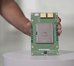
"A0 silicon" is the first batch of chips that come back from the foundry after the tapeout. It's a prototype that is likely circulated within Intel internally, and to a very exclusive group of ISVs and industry partners, under very strict NDAs. It is common practice to ship prototypes with significantly lower clock speeds than what the silicon is capable of, at least to the ISVs, so they can test for functionality and begin developing software for the silicon.


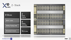
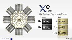
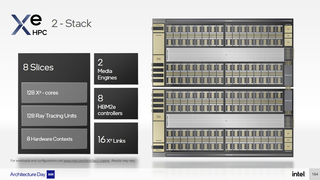
Our math for the clock speed is as follows. Intel, in the presentation mentions that each package (OAM) puts out a throughput of 32,768 FP32 ops per clock cycle. It also says that a 2-stack (one package) amounts to 128 Xe-cores, and that each Xe HPC core Vector Engine offers 256 FP32 ops per clock cycle. These add up to 32,768 FP32 ops/clock for one package (a 2-stack). From here, we calculate that 45,000 GFLOPs (measured in clpeak by the way), divided by 32,768 FP32 ops/clock, amounts to 1373 MHz clock speed. A production stepping will likely have higher clock speeds, and throughput scales linearly, but even 1.37 GHz seems like a number Intel could finalize on, given the sheer size and "weight" (power draw) of the silicon (rumored to be 600 W for A0). All this power comes with great thermal costs, with Intel requiring liquid cooling for the OAMs. If these numbers can make it into the final product, then Intel has very well broken through into the HPC space in a big way.


View at TechPowerUp Main Site
 
Last edited:
1629487627436.png


This picture is a pretty big deal if Intel is being honest about the architecture.

Xe-link is probably not a crossbar as indicated in the picture (I'm assuming its closer to a CLOS network or Benes Network). But the idea is that a switch can provide an any-to-any connection at full speed between all nodes. If they're really using a good switching fabric and can provide full throughput between all nodes, then they're going to be a worthy competitor against NVidia's NVLink technology.
 

Unlikely. NVidia is spec'd out for 600GBps per link (that's 4800 Gbit/s). If Intel is seriously trying to compete against NVLink, I'd be expecting at least 50 GBps (400 Gbit) throughput link-to-link, or more.

Coming in at 1/12th the speed of NVidia is fine for a 1st gen product, but they'll have to catch up quickly after proving themselves. The speeds of these links are an order of magnitude more bandwidth than what even InfiniBand offers.
 
Xe-link is probably not a crossbar as indicated in the picture (I'm assuming its closer to a CLOS network or Benes Network). But the idea is that a switch can provide an any-to-any connection at full speed between all nodes. If they're really using a good switching fabric and can provide full throughput between all nodes, then they're going to be a worthy competitor against NVidia's NVLink technology.

yqut7b1tln.jpg

I'd interpret this slide as "crossbar"
 
At 600 watts? How do they compare per unite of measurement (TFLOPs per watt)?
 
Wish Intel is preparing good software development environment stack to support this in the long run
 
At 600 watts? How do they compare per unite of measurement (TFLOPs per watt)?
Outside has calculations how will be performance if PV work at 2GHz... maybe 600 watts target is for device when work on frequency above of this sample which is on early silicon.
 
:D Soo... Can it run Crysis? :D
 
yqut7b1tln.jpg

I'd interpret this slide as "crossbar"

Thanks for the slide.

Unfortunately, its giving me more questions rather than answers. The ArchDay21claims site doesn't provide details (https://edc.intel.com/content/www/us/en/products/performance/benchmarks/architecture-day-2021/). I don't know if that's 90 Gbit/sec or if its 90 GByte/sec for example.

8x links gets us to 720 "G" per second, hopefully that's "GBytes" which would be a bit faster than NVSwitch and competitive. But if its "Gbits", then that's only 90GByte/sec (which is probably passable, but much slower than NVidia). Its "passable" because 16x PCIe 4 is just 32GByte/sec, so really, anything "faster than PCIe" is kind of a win. But I'm assuming Intel is aiming at the big boy, the A100 600GByte/sec fabric.

------

Note: most "crossbars" are just nonblocking CLOS networks. :) I think people use the term "crossbar" as shorthand for a "switch that has no restriction on bandwidth" (which a nonblocking CLOS network qualifies), and not necessarily a "physical crossbar" (which takes up O(n^2 space), while CLOS network is O(n*log(n)) space)
 
Last edited:
Sure it does. Also, where's the chiller hiding? LOLtel really earning their name (and using tsmc makes it even better).
 
View attachment 213480

This picture is a pretty big deal if Intel is being honest about the architecture.

Xe-link is probably not a crossbar as indicated in the picture (I'm assuming its closer to a CLOS network or Benes Network). But the idea is that a switch can provide an any-to-any connection at full speed between all nodes. If they're really using a good switching fabric and can provide full throughput between all nodes, then they're going to be a worthy competitor against NVidia's NVLink technology.
That's bit a crossbar. That's a fully connected topology, as every node has a link to another node. You can see it in W1zzard post that each of them has 8 links. It doesn't need any switch at all, there are dedicated links from each node to all other nodes.
 
Much glue.
 
Mi300 announcements is near
And availability before ponte vecchio

With 70-75 tflops FP32 ....
exactly -- this is pure shareholder hype.
 
Probably good enough to push bundle's.
 
at 600w redundant psu's might be needed.
 
huh, isn't the RTX3090 already capable of ~36 TFLOPS of FP32 at 350W TGP, what's so special about a MCM solution getting 45 TFLOPS at 600W LMAO.
 
FP64 is 1:1 FP32. So its FP64 throughput is identical.

Are you sure? Most of the time, FP64 is 1:2 FP32 (half-speed).

AVX512, A100, MI100, etc. etc. All the same. If you double the bits, you double the ram-bandwidth needed and therefore half the speed (100 64-bit numbers is 800 bytes. 100x32-bit numbers is just 400 bytes).

Since RAM is moving effectively at half speed, it "just makes sense" for compute to also move at 1/2 speed.
 
huh, isn't the RTX3090 already capable of ~36 TFLOPS of FP32 at 350W TGP, what's so special about a MCM solution getting 45 TFLOPS at 600W LMAO.
100000 ways was repeated Nvidia lie with this number. Real teraflops is 1/2 from advertising teraflops.
 
huh, isn't the RTX3090 already capable of ~36 TFLOPS of FP32 at 350W TGP, what's so special about a MCM solution getting 45 TFLOPS at 600W LMAO.

NVidia A100 (the $10,000 server card) is only 19.5 FP32 TFlops: https://www.nvidia.com/content/dam/en-zz/Solutions/Data-Center/a100/pdf/nvidia-a100-datasheet.pdf

And only 9.7 FP64 TFlops.

The Tensor-flops are an elevated number that only deep-learning folk care about (and apparently not all deep learning folk are using those tensor cores). Achieving ~20 FP32 TFlops general-purpose code is basically the best today (MI100 is a little bit faster, but without as much of that NVlink thing going on).

So 45 TFlops of FP32 is pretty huge by today's standards. However, Intel is going to be competing against the next-generation products, not the A100. I'm sure NVidia is going to grow, but 45TFlops per card is probably going to be competitive.

That's bit a crossbar. That's a fully connected topology, as every node has a link to another node. You can see it in W1zzard post that each of them has 8 links. It doesn't need any switch at all, there are dedicated links from each node to all other nodes.

Fully connected is stupid. It means that of the 720 G (bit? Byte?) available to Node A (90 G x 8 connections in NodeA), but you only have 90G wired between Node A and Node B. Which means, Node A and B can only ever talk at 90G speeds.

What if Node B has all of the data that's important for the calculation? Well, you'd like it if NodeA can communicate at 720 G (byte/sec ??) with Node B. You have 8x SerDes after all, it'd be nice to "gang up" those Serdes and have them work together.

Both a crossbar and a CLOS network would allow that. A fully connected topology cannot. This is the difference between Zen1 and Zen2, where Zen2 has a switch (probably a CLOS network, might be a crossbar) efficiently allocating RAM to all 8-nodes. Zen1 was fully connected (Node 1 had a high speed connection to Node 2, Node 3, and Node 4).

That switch is in fact, a big deal, and the key to scalability.
 
Last edited:
Back
Top