- Joined
- Aug 19, 2017
- Messages
- 2,652 (0.99/day)
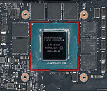
When NVIDIA announced the appearance of the GeForce RTX 3080 Ti mobile graphics card, we were left with a desire to see just what the GA103 silicon powering the GPU looks like. And thanks to the Chinese YouTuber Geekerwan, we have the first pictures of the GPU. Pictured below is GA103S/GA103M SKU with GN20-E8-A1 labeling. It features 58 SMs that make up for 7424 CUDA cores in total. The number of Tensor cores for this SKU is set to 232, while there are 58 RT cores. NVIDIA has decided to pair this GPU with a 256-bit memory bus and 16 GB GDDR6 memory.
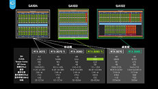
As it turns out, the full GA103 silicon has a total of 7680 CUDA cores and a 320-bit memory bus, so this mobile version is a slightly cut-down variant. It sits perfectly between GA104 and GA102 SKUs, providing a significant improvement to the core count of GA104 silicon. Power consumption of the GA103 SKU for GeForce RTX 3080 Ti mobile is set to a variable 80-150 Watt range, which can be adjusted according to the system's cooling capacity. An interesting thing to point out is a die size of 496 mm², which is a quarter more significant compared to GA104, for a quarter higher number of CUDA cores.


View at TechPowerUp Main Site
As it turns out, the full GA103 silicon has a total of 7680 CUDA cores and a 320-bit memory bus, so this mobile version is a slightly cut-down variant. It sits perfectly between GA104 and GA102 SKUs, providing a significant improvement to the core count of GA104 silicon. Power consumption of the GA103 SKU for GeForce RTX 3080 Ti mobile is set to a variable 80-150 Watt range, which can be adjusted according to the system's cooling capacity. An interesting thing to point out is a die size of 496 mm², which is a quarter more significant compared to GA104, for a quarter higher number of CUDA cores.


View at TechPowerUp Main Site


