- Joined
- Oct 9, 2007
- Messages
- 47,205 (7.55/day)
- Location
- Hyderabad, India
| System Name | RBMK-1000 |
|---|---|
| Processor | AMD Ryzen 7 5700G |
| Motherboard | ASUS ROG Strix B450-E Gaming |
| Cooling | DeepCool Gammax L240 V2 |
| Memory | 2x 8GB G.Skill Sniper X |
| Video Card(s) | Palit GeForce RTX 2080 SUPER GameRock |
| Storage | Western Digital Black NVMe 512GB |
| Display(s) | BenQ 1440p 60 Hz 27-inch |
| Case | Corsair Carbide 100R |
| Audio Device(s) | ASUS SupremeFX S1220A |
| Power Supply | Cooler Master MWE Gold 650W |
| Mouse | ASUS ROG Strix Impact |
| Keyboard | Gamdias Hermes E2 |
| Software | Windows 11 Pro |
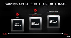
Way back in January 2021, we heard a spectacular rumor about "Navi 31," the next-generation big GPU by AMD, being the company's first logic-MCM GPU (a GPU with more than one logic die). The company has a legacy of MCM GPUs, but those have been a single logic die surrounded by memory stacks. The RDNA3 graphics architecture that the "Navi 31" is based on, sees AMD fragment the logic die into smaller chiplets, with the goal of ensuring that only those specific components that benefit from the TSMC N5 node (6 nm), such as the number crunching machinery, are built on the node, while ancillary components, such as memory controllers, display controllers, or even media accelerators, are confined to chiplets built on an older node, such as the TSMC N6 (6 nm). AMD had taken this approach with its EPYC and Ryzen processors, where the chiplets with the CPU cores got the better node, and the other logic components got an older one.
Greymon55 predicts an interesting division of labor on the "Navi 31" MCM. Apparently, the number-crunching machinery is spread across two GCD (Graphics Complex Dies?). These dies pack the Shader Engines with their RDNA3 compute units (CU), Command Processor, Geometry Processor, Asynchronous Compute Engines (ACEs), Rendering Backends, etc. These are things that can benefit from the advanced 5 nm node, enabling AMD to the CUs at higher engine clocks. There's also sound logic behind building a big GPU with two such GCDs instead of a single large GCD, as smaller GPUs can be made with a single such GCD (exactly why we have two 8-core chiplets making up a 16-core Ryzen processors, and the one of these being used to create 8-core and 6-core SKUs). The smaller GCD would result in better yields per wafer, and minimize the need for separate wafer orders for a larger die (such as in the case of the Navi 21).

Besides two GCDs, there are four MCDs (memory controller dies). Greymon55 predicts that these could be built on the 6 nm (TSMC N6) node, a slightly more advanced node than N7 (7 nm). Each MCD controls two 32-bit memory paths, controlling two memory chips, or 64-bit of the memory bus width. Four such MCDs make up 256-bit. For ASICs with just one GCD, there could be three MCDs (192-bit), or even just two (128-bit). The MCD packs the GDDR6 memory controller, as well as its PHY. There could also be exotic fixed-function hardware for features such as memory compression and ECC (latter being available on Pro SKUs).
The third and final kind of die is the I/O Die. On both Socket AM4 and SP3 processors, the IOD serves as town-square, connecting all the CPU chiplets, and crams memory, PCIe, and other platform I/O. On "Navi 31," the IOD could pack all the components that never need overclocking—these include the PCI-Express switch (which connects the GPU to the system), the Display CoreNext (DCN) component that controls the various display outputs; and perhaps even the Video CoreNext (VCN), which packs the media accelerators. At this point it's not known which node the IOD is built on.
The ether connecting all 7 chiplets on the "Navi 31" MCM is Infinity Fabric. IFOP (Infinity Fabric over package), as implemented on EPYC "Milan" or the upcoming "Genoa" processors, has shown that its wiring isn't of high enough density that it needs an interposer, and can make do with the fiberglass substrate. Such will be the case with "Navi 31," too. The MCDs will wire out to the GDDR6 memory devices just the way current GPUs do it, so will the IOD, while all the chiplets talk to each other over IFOP.
View at TechPowerUp Main Site | Source
Greymon55 predicts an interesting division of labor on the "Navi 31" MCM. Apparently, the number-crunching machinery is spread across two GCD (Graphics Complex Dies?). These dies pack the Shader Engines with their RDNA3 compute units (CU), Command Processor, Geometry Processor, Asynchronous Compute Engines (ACEs), Rendering Backends, etc. These are things that can benefit from the advanced 5 nm node, enabling AMD to the CUs at higher engine clocks. There's also sound logic behind building a big GPU with two such GCDs instead of a single large GCD, as smaller GPUs can be made with a single such GCD (exactly why we have two 8-core chiplets making up a 16-core Ryzen processors, and the one of these being used to create 8-core and 6-core SKUs). The smaller GCD would result in better yields per wafer, and minimize the need for separate wafer orders for a larger die (such as in the case of the Navi 21).

Besides two GCDs, there are four MCDs (memory controller dies). Greymon55 predicts that these could be built on the 6 nm (TSMC N6) node, a slightly more advanced node than N7 (7 nm). Each MCD controls two 32-bit memory paths, controlling two memory chips, or 64-bit of the memory bus width. Four such MCDs make up 256-bit. For ASICs with just one GCD, there could be three MCDs (192-bit), or even just two (128-bit). The MCD packs the GDDR6 memory controller, as well as its PHY. There could also be exotic fixed-function hardware for features such as memory compression and ECC (latter being available on Pro SKUs).
The third and final kind of die is the I/O Die. On both Socket AM4 and SP3 processors, the IOD serves as town-square, connecting all the CPU chiplets, and crams memory, PCIe, and other platform I/O. On "Navi 31," the IOD could pack all the components that never need overclocking—these include the PCI-Express switch (which connects the GPU to the system), the Display CoreNext (DCN) component that controls the various display outputs; and perhaps even the Video CoreNext (VCN), which packs the media accelerators. At this point it's not known which node the IOD is built on.
The ether connecting all 7 chiplets on the "Navi 31" MCM is Infinity Fabric. IFOP (Infinity Fabric over package), as implemented on EPYC "Milan" or the upcoming "Genoa" processors, has shown that its wiring isn't of high enough density that it needs an interposer, and can make do with the fiberglass substrate. Such will be the case with "Navi 31," too. The MCDs will wire out to the GDDR6 memory devices just the way current GPUs do it, so will the IOD, while all the chiplets talk to each other over IFOP.
View at TechPowerUp Main Site | Source


