- Joined
- Oct 9, 2007
- Messages
- 47,231 (7.55/day)
- Location
- Hyderabad, India
| System Name | RBMK-1000 |
|---|---|
| Processor | AMD Ryzen 7 5700G |
| Motherboard | ASUS ROG Strix B450-E Gaming |
| Cooling | DeepCool Gammax L240 V2 |
| Memory | 2x 8GB G.Skill Sniper X |
| Video Card(s) | Palit GeForce RTX 2080 SUPER GameRock |
| Storage | Western Digital Black NVMe 512GB |
| Display(s) | BenQ 1440p 60 Hz 27-inch |
| Case | Corsair Carbide 100R |
| Audio Device(s) | ASUS SupremeFX S1220A |
| Power Supply | Cooler Master MWE Gold 650W |
| Mouse | ASUS ROG Strix Impact |
| Keyboard | Gamdias Hermes E2 |
| Software | Windows 11 Pro |
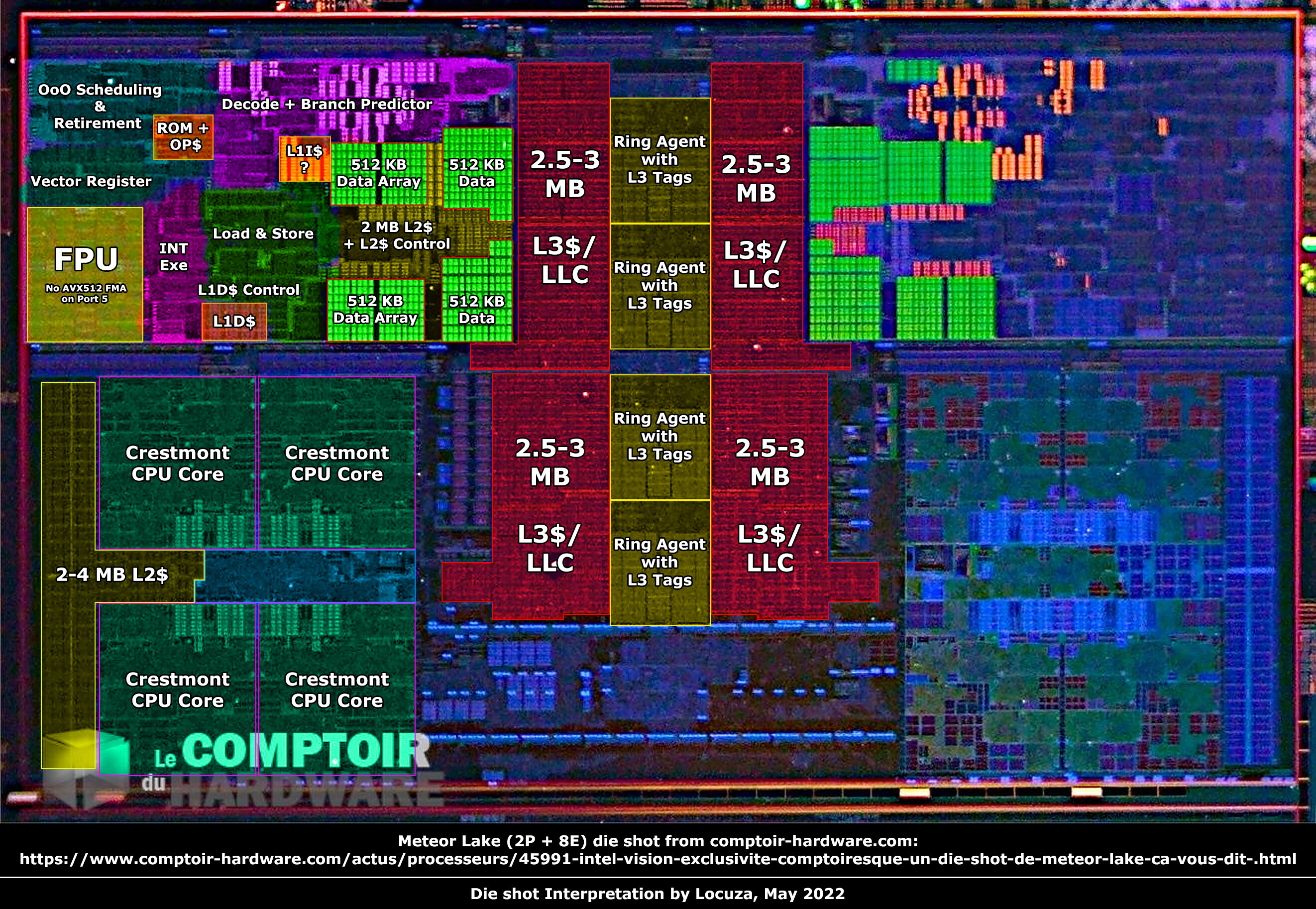
Intel's next-generation "Meteor Lake" processor is the first mass-production client processor to embody the company's IDM 2.0 manufacturing strategy—one of building processors with multiple logic tiles interconnected with Foveros and a base-tile (essentially an interposer). Each tile is built on a silicon fabrication process most suitable to it, so that the most advanced node could be reserved for the component that benefits from it the most. For example, while you need the SIMD components of the iGPU to be built on an advanced low-power node, you don't need its display controller and media engine to, and these could be relegated to a tile built on a less advanced node. This way Intel is able to maximize its use of wafers for the most advanced nodes in a graded fashion.
Japanese tech publication PC Watch has annotated the "Meteor Lake" SoC, and points out that the vast majority of the chip's tiles and logic die-area is manufactured on TSMC nodes. The MCM consists of four logic tiles—the CPU tile, the Graphics tile, the SoC tile, and the I/O tile. The four sit on a base tile that facilitates extreme-density microscopic wiring interconnecting the logic tiles. The base tile is built on the 22 nm HKMG silicon fabrication node. This tile lacks any logic, and only serves to interconnect the tiles. Intel has an active 22 nm node, and decided it has the right density for the job.


The CPU tile is the only logic tile built on an Intel node, which in this case is the Intel 4 node. The company considers this process to be on-par or better than TSMC's N5, and it probably wanted the crown jewels of its IP—CPU cores—to be built on a native fab. The CPU tile contains the CPU cores, a last-level cache, and Foveros interfaces.
The Graphics tile is the second-most important logic tile, and contains an iGPU based on the Xe-LPG graphics architecture. An evolution of Xe-LP, the LPG features real-time ray tracing capabilities. Intel decided to use the TSMC N5 (5 nm EUV) node for this tile. Not all of the iGPU is based on this tile, some of it, such as the Display Engine, could be located on the I/O tile.
The SoC tile is the largest in terms of area, and is built on the TSMC N6 (6 nm) node. This contains the memory controllers, PCIe root-complex, and the controllers and SerDes (serializer-deserializer) of the various on-package devices. The I/O die is the smallest die, and is essentially an extension of the SoC die. It's built on the same TSMC N6 node, and features the PHY (physical layer) components of the various I/O.
View at TechPowerUp Main Site | Source
Japanese tech publication PC Watch has annotated the "Meteor Lake" SoC, and points out that the vast majority of the chip's tiles and logic die-area is manufactured on TSMC nodes. The MCM consists of four logic tiles—the CPU tile, the Graphics tile, the SoC tile, and the I/O tile. The four sit on a base tile that facilitates extreme-density microscopic wiring interconnecting the logic tiles. The base tile is built on the 22 nm HKMG silicon fabrication node. This tile lacks any logic, and only serves to interconnect the tiles. Intel has an active 22 nm node, and decided it has the right density for the job.


The CPU tile is the only logic tile built on an Intel node, which in this case is the Intel 4 node. The company considers this process to be on-par or better than TSMC's N5, and it probably wanted the crown jewels of its IP—CPU cores—to be built on a native fab. The CPU tile contains the CPU cores, a last-level cache, and Foveros interfaces.
The Graphics tile is the second-most important logic tile, and contains an iGPU based on the Xe-LPG graphics architecture. An evolution of Xe-LP, the LPG features real-time ray tracing capabilities. Intel decided to use the TSMC N5 (5 nm EUV) node for this tile. Not all of the iGPU is based on this tile, some of it, such as the Display Engine, could be located on the I/O tile.
The SoC tile is the largest in terms of area, and is built on the TSMC N6 (6 nm) node. This contains the memory controllers, PCIe root-complex, and the controllers and SerDes (serializer-deserializer) of the various on-package devices. The I/O die is the smallest die, and is essentially an extension of the SoC die. It's built on the same TSMC N6 node, and features the PHY (physical layer) components of the various I/O.
View at TechPowerUp Main Site | Source


