TheLostSwede
News Editor
- Joined
- Nov 11, 2004
- Messages
- 18,373 (2.46/day)
- Location
- Sweden
| System Name | Overlord Mk MLI |
|---|---|
| Processor | AMD Ryzen 7 7800X3D |
| Motherboard | Gigabyte X670E Aorus Master |
| Cooling | Noctua NH-D15 SE with offsets |
| Memory | 32GB Team T-Create Expert DDR5 6000 MHz @ CL30-34-34-68 |
| Video Card(s) | Gainward GeForce RTX 4080 Phantom GS |
| Storage | 1TB Solidigm P44 Pro, 2 TB Corsair MP600 Pro, 2TB Kingston KC3000 |
| Display(s) | Acer XV272K LVbmiipruzx 4K@160Hz |
| Case | Fractal Design Torrent Compact |
| Audio Device(s) | Corsair Virtuoso SE |
| Power Supply | be quiet! Pure Power 12 M 850 W |
| Mouse | Logitech G502 Lightspeed |
| Keyboard | Corsair K70 Max |
| Software | Windows 10 Pro |
| Benchmark Scores | https://valid.x86.fr/yfsd9w |
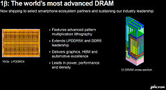
Micron Technology, Inc., announced today that it is shipping qualification samples of its 1β (1-beta) DRAM technology to select smartphone manufacturers and chipset partners and has achieved mass production readiness with the world's most advanced DRAM technology node. The company is debuting its next generation of process technology on its low-power double data rate 5X (LPDDR5X) mobile memory, delivering top speed grades of 8.5 gigabits (Gb) per second. The node delivers significant gains across performance, bit density and power efficiency that will have sweeping market benefits. Beyond mobile, 1β delivers the low-latency, low-power, high-performance DRAM that is essential to support highly responsive applications, real-time services, personalization and contextualization of experiences, from intelligent vehicles to data centers.
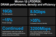
The world's most advanced DRAM process node, 1β represents an advancement of the company's market leadership cemented with the volume shipment of 1α (1-alpha) in 2021. The node delivers around a 15% power efficiency improvement and more than a 35% bit density improvement with a 16Gb per die capacity. "The launch of our 1-beta DRAM signals yet another leap forward for memory innovation, brought to life by our proprietary multi-patterning lithography in combination with leading-edge process technology and advanced materials capabilities," said Scott DeBoer, executive vice president of technology and products at Micron. "In delivering the world's most advanced DRAM technology with more bits per memory wafer than ever before, this node lays the foundation to usher in a new generation of data-rich, intelligent and energy-efficient technologies from the edge to the cloud."
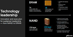
This milestone also follows quickly on the heels of Micron's shipment of the world's first 232-layer NAND in July, architected to drive unprecedented performance and areal density for storage. With these new firsts, Micron continues to set the pace for the market across memory and storage innovations—both made possible by the company's deep roots in cutting-edge research and development (R&D) and manufacturing process technology.
With sampling of LPDDR5X, the mobile ecosystem will be the first to reap the benefits of 1β DRAM's significant gains, which will unlock next-generation mobile innovation and advanced smartphone experiences—all while consuming less power. With 1β's speed and density, high-bandwidth use cases will be responsive and smooth during downloads, launches and simultaneous use of data-hungry 5G and artificial intelligence (AI) applications. Additionally, 1β-based LPDDR5X will not only enhance smartphone camera launch, night mode and portrait mode with speed and clarity, but it will enable shake-free, high-resolution 8K video recording and intuitive in-phone video editing.
The low power per bit consumption of 1β process technology delivers the most power-efficient memory technology on the market for smartphones yet. This allows smartphone manufacturers to design devices with more efficient battery life—crucial as consumers look to prolong their batteries while using energy-draining, data-intensive apps.
The power savings are also enabled by the implementation of new JEDEC enhanced dynamic voltage and frequency scaling extensions core (eDVFSC) techniques on this 1β-based LPDDR5X. The addition of eDVFSC at a doubled frequency tier of up to 3,200 megabits per second provides improved power savings controls to enable more efficient use of power based off unique end user patterns.
Micron challenges laws of physics with sophisticated lithography and nanomanufacturing
Micron's industry-first 1β node allows higher memory capacity in a smaller footprint—enabling lower cost per bit of data. DRAM scaling has largely been defined by this ability to deliver more and faster memory per square millimeter of semiconductor area, which requires shrinking the circuits to fit billions of memory cells on a chip roughly the size of a fingernail. With each process node, the semiconductor industry has been shrinking devices every year or two for decades; however, as chips have grown smaller, defining circuit patterns on wafers requires challenging the laws of physics.
While the industry has begun to shift to a new tool that uses extreme ultraviolet light to overcome these technical challenges, Micron has tapped into its proven leading-edge nanomanufacturing and lithography prowess to bypass this still emergent technology. Doing so involves applying the company's proprietary, advanced multi-patterning techniques and immersion capabilities to pattern these miniscule features with the highest precision. The greater capacity delivered by this reduction will also enable devices with small form factors, such as smartphones and IoT devices, to fit more memory into compact footprints.
To achieve its competitive edge with 1β and 1α, Micron has also aggressively advanced its manufacturing excellence, engineering capabilities and pioneering R&D over the past several years. This accelerated innovation first enabled Micron's unprecedented ramp of its 1α node one year ahead of its competition, which established Micron's leadership in both DRAM and NAND for the first time in the company's history. Over the years, Micron has further invested billions of dollars in transforming its fabs into leading-edge, highly automated, sustainable and AI-driven facilities. This includes investments in Micron's plant in Hiroshima, Japan, which will be mass producing DRAM on 1β.
1-beta lays ubiquitous foundation for a more interconnected, sustainable world
As energy-sapping use cases like machine-to-machine communications, AI and machine learning take flight, power-efficient technologies are an increasingly critical need for businesses, especially those looking to meet strict sustainability targets and reduce operating expenses. Researchers have found that training a single AI model can emit five times the lifetime carbon emissions of an American car, including its manufacture. Further, information and communication technology is already predicted to use 20% of the world's electricity by 2030.
Micron's 1β DRAM node provides a versatile foundation to power advancements in a connected world that needs fast, ubiquitous, energy-efficient memory to fuel digitization, optimization and automation. The high-density, low-power memory fabricated on 1β enables more energy-efficient flow of data between data-hungry smart things, systems and applications, and more intelligence from edge to cloud. Over the next year, the company will begin to ramp the rest of its portfolio on 1β across embedded, data center, client, consumer, industrial and automotive segments, including graphics memory, high-bandwidth memory and more.
View at TechPowerUp Main Site | Source
The world's most advanced DRAM process node, 1β represents an advancement of the company's market leadership cemented with the volume shipment of 1α (1-alpha) in 2021. The node delivers around a 15% power efficiency improvement and more than a 35% bit density improvement with a 16Gb per die capacity. "The launch of our 1-beta DRAM signals yet another leap forward for memory innovation, brought to life by our proprietary multi-patterning lithography in combination with leading-edge process technology and advanced materials capabilities," said Scott DeBoer, executive vice president of technology and products at Micron. "In delivering the world's most advanced DRAM technology with more bits per memory wafer than ever before, this node lays the foundation to usher in a new generation of data-rich, intelligent and energy-efficient technologies from the edge to the cloud."


This milestone also follows quickly on the heels of Micron's shipment of the world's first 232-layer NAND in July, architected to drive unprecedented performance and areal density for storage. With these new firsts, Micron continues to set the pace for the market across memory and storage innovations—both made possible by the company's deep roots in cutting-edge research and development (R&D) and manufacturing process technology.
With sampling of LPDDR5X, the mobile ecosystem will be the first to reap the benefits of 1β DRAM's significant gains, which will unlock next-generation mobile innovation and advanced smartphone experiences—all while consuming less power. With 1β's speed and density, high-bandwidth use cases will be responsive and smooth during downloads, launches and simultaneous use of data-hungry 5G and artificial intelligence (AI) applications. Additionally, 1β-based LPDDR5X will not only enhance smartphone camera launch, night mode and portrait mode with speed and clarity, but it will enable shake-free, high-resolution 8K video recording and intuitive in-phone video editing.
The low power per bit consumption of 1β process technology delivers the most power-efficient memory technology on the market for smartphones yet. This allows smartphone manufacturers to design devices with more efficient battery life—crucial as consumers look to prolong their batteries while using energy-draining, data-intensive apps.
The power savings are also enabled by the implementation of new JEDEC enhanced dynamic voltage and frequency scaling extensions core (eDVFSC) techniques on this 1β-based LPDDR5X. The addition of eDVFSC at a doubled frequency tier of up to 3,200 megabits per second provides improved power savings controls to enable more efficient use of power based off unique end user patterns.
Micron challenges laws of physics with sophisticated lithography and nanomanufacturing
Micron's industry-first 1β node allows higher memory capacity in a smaller footprint—enabling lower cost per bit of data. DRAM scaling has largely been defined by this ability to deliver more and faster memory per square millimeter of semiconductor area, which requires shrinking the circuits to fit billions of memory cells on a chip roughly the size of a fingernail. With each process node, the semiconductor industry has been shrinking devices every year or two for decades; however, as chips have grown smaller, defining circuit patterns on wafers requires challenging the laws of physics.
While the industry has begun to shift to a new tool that uses extreme ultraviolet light to overcome these technical challenges, Micron has tapped into its proven leading-edge nanomanufacturing and lithography prowess to bypass this still emergent technology. Doing so involves applying the company's proprietary, advanced multi-patterning techniques and immersion capabilities to pattern these miniscule features with the highest precision. The greater capacity delivered by this reduction will also enable devices with small form factors, such as smartphones and IoT devices, to fit more memory into compact footprints.
To achieve its competitive edge with 1β and 1α, Micron has also aggressively advanced its manufacturing excellence, engineering capabilities and pioneering R&D over the past several years. This accelerated innovation first enabled Micron's unprecedented ramp of its 1α node one year ahead of its competition, which established Micron's leadership in both DRAM and NAND for the first time in the company's history. Over the years, Micron has further invested billions of dollars in transforming its fabs into leading-edge, highly automated, sustainable and AI-driven facilities. This includes investments in Micron's plant in Hiroshima, Japan, which will be mass producing DRAM on 1β.
1-beta lays ubiquitous foundation for a more interconnected, sustainable world
As energy-sapping use cases like machine-to-machine communications, AI and machine learning take flight, power-efficient technologies are an increasingly critical need for businesses, especially those looking to meet strict sustainability targets and reduce operating expenses. Researchers have found that training a single AI model can emit five times the lifetime carbon emissions of an American car, including its manufacture. Further, information and communication technology is already predicted to use 20% of the world's electricity by 2030.
Micron's 1β DRAM node provides a versatile foundation to power advancements in a connected world that needs fast, ubiquitous, energy-efficient memory to fuel digitization, optimization and automation. The high-density, low-power memory fabricated on 1β enables more energy-efficient flow of data between data-hungry smart things, systems and applications, and more intelligence from edge to cloud. Over the next year, the company will begin to ramp the rest of its portfolio on 1β across embedded, data center, client, consumer, industrial and automotive segments, including graphics memory, high-bandwidth memory and more.
View at TechPowerUp Main Site | Source


 In all seriousness though, all I can see is a segmented die with a series of repeated memory arrays. What would stand in the way of just having 25% less in one implementation?
