• Welcome to TechPowerUp Forums, Guest! Please check out our forum guidelines for info related to our community.

Tom's editorial on Arrow lake "big gains in productivity and power efficiency, but not in gaming"

Joined
Jun 1, 2011
Messages
4,977 (0.97/day)
Location
in a van down by the river
Processor faster at instructions than yours
Motherboard more nurturing than yours
Cooling frostier than yours
Memory superior scheduling & haphazardly entry than yours
Video Card(s) better rasterization than yours
Storage more ample than yours
Display(s) increased pixels than yours
Case fancier than yours
Audio Device(s) further audible than yours
Power Supply additional amps x volts than yours
Mouse without as much gnawing as yours
Keyboard less clicky than yours
VR HMD not as odd looking as yours
Software extra mushier than yours
Benchmark Scores up yours
Maybe not for headline gaming peak performance numbers, but both AMD and Intel have often had 'best band for buck' gaming products that sit in the middle of the product stack, e.g. Ryzen 5600X or i5-12600K, where anything beyond that point is diminishing returns (usually because the increased power use / TDP starts imposing performance limiting or the base platform not being able to exploit the extra core bandwidth).

I'm expecting the Arrow Lake platform to move that performance point forward for gamers, so not a massive waste of time in that sense - primarily because the IPC/IPS vs TDP is going to be a lot better thus not butting up against those limits quite as soon. Effectively, more cores maybe maintaining a better frequency for less power use/wastage means that average baseline gaming performance will be higher.

So basically, outside of the X3D chips, and the 14900K's, etc., this might make Intel more of a mid-low end default gamers choice.
 
this might make Intel more of a mid-low end default gamers choice.
I'm hoping for great value. I cheer on both sides, competitive markets equal lower prices ( as long as they are not in collusion)
 
I'm hoping for great value. I cheer on both sides, competitive markets equal lower prices ( as long as they are not in collusion)
Maybe... I expect AM5 price reductions if overlapping product segment performance favours Intel and they have chosen similar/matching/slightly lower MSRPs...
 
My only question at this point on 285K is does it overclock? The 14th gen was pegged out already and had huge power draws by default, so the fact that they've dropped the power draw (and temps) may mean that there's some headroom there?

I also noticed that the 14900k was tested in gaming benchmarks in baseline performance mode (which is a 125W-PL1, 188W-PL2 limited profile?) even though their own table they published for "Intel Recommendations: 'Intel Default Settings'" says "Intel recommends using the 'Extreme' Power Delivery Profile if supported by the voltage regulator and motherboard design", which would actually be the 253W-limit for 14900k. It even says "Intel does not recommend Baseline power delivery profiles for 13th and 14th Gen K Sku processors unless required for compatibility".
1728575165678.png


Maybe I'm missing something, but that certainly seems pretty shady...it may explain why the 14900k numbers they posted are lower than the review numbers for it.
Edit: Digging through https://edc.intel.com/content/www/u...marks/intel-core-ultra-processors-series-2_1/, it looks like they set the 14900k at PL1=PL2=253W for their benchmark tests and the 285K was at 250W...but they did their power efficiency tests with the 285K set at 125W and the 14900k at 253W lol
 
Last edited:
@R0H1T , this and many other things hopefully will be covered when reviewed - especially if @W1zzard (or whoever reviews it) does the normal efficiency charts.

With Raptor Lake performance scaled pretty poorly as PL was raised upto and past 200W - it may still be a similar story for Arrow Lake in terms of being in the 200W zone, however potentially they may have better scaling from the 100-150W power window compared to Raptor Lake (which locked to lower <95W power limits was actually pretty efficient especially considering Intel 7/10nm process - which is why in terms of bang for buck the Core i3 Alder/Raptor lake CPUs were not pure trash).
 
They can call a silicon Interposer whatever they like but AMD did it first....
 
My only question at this point on 285K is does it overclock? The 14th gen was pegged out already and had huge power draws by default, so the fact that they've dropped the power draw (and temps) may mean that there's some headroom there?

I also noticed that the 14900k was tested in gaming benchmarks in baseline performance mode (which is a 125W-PL1, 188W-PL2 limited profile?) even though their own table they published for "Intel Recommendations: 'Intel Default Settings'" says "Intel recommends using the 'Extreme' Power Delivery Profile if supported by the voltage regulator and motherboard design", which would actually be the 253W-limit for 14900k. It even says "Intel does not recommend Baseline power delivery profiles for 13th and 14th Gen K Sku processors unless required for compatibility".
View attachment 366971

Maybe I'm missing something, but that certainly seems pretty shady...it may explain why the 14900k numbers they posted are lower than the review numbers for it.
Edit: Digging through https://edc.intel.com/content/www/u...marks/intel-core-ultra-processors-series-2_1/, it looks like they set the 14900k at PL1=PL2=253W for their benchmark tests and the 285K was at 250W...but they did their power efficiency tests with the 285K set at 125W and the 14900k at 253W lol
Just like AMD it's node process limited. The thermal density they have a upper hand with a thinner IHS I'm sure. Putting Ecores between P cores to further enhance Delta was a good move too.
 
Honestly, probably a good trade off for the majority of the market. Gaming performance is really relevant to a very small portion of the market, most people will be GPU limited and I don’t think that many are going to see the 600 to 700 FPS increase in their CS matches. Just a hunch. Better MT performance and energy efficiency are universally useful though.
 
You're comparing the foveros to AMD chiplet or something else?

2017 AMD was using a silicon interposer.

As much hate/dislike/distain anyone may have they did a LOT first and have moved the needle for consumers.
Here are their firsts.

Tessellation
GPU compute
X64
Chiplet
Interposer
3D stacking
HBM
SSD on GPU
HDR


Intel was the pioneer of HT/SMT. They have made huge advances in paying off companies in monopolistic practices and been fined a pittance for trying to eliminate competitive companies. Nvidia has a great PR and spin team and a lot of money.
 

It goes a couple of years further back to the original R9 GPUs which had the first HBM memory, e.g. R9 Nano. Vega wasn't the first, but AMD were the first to do it in that way... I just wish it was more successful in terms of the actual product. In practice the approach has many benefits which is why Intel have gone all in - probably because they have better resources to - a shame AMD haven't been able to leverage it in the same way but I guess the post-Athlon64 / pre-Ryzen years prohibited such moves.

BUT.... whilst innovative and certainly pushing tech forward thanks to integrating the seperate dies into one physical block unit (and not just seperate dies sharing an interposer), it's not exactly a new general idea - the seperate dies are still interconnected with their own interposer, so it's an interconnecting block on top of another interconnecting block.

As much hate/dislike/distain anyone may have they did a LOT first and have moved the needle for consumers.
Here are their firsts.

Tessellation
GPU compute
X64
Chiplet
Interposer

3D stacking
HBM
SSD on GPU
HDR


Intel was the pioneer of HT/SMT. They have made huge advances in paying off companies in monopolistic practices and been fined a pittance for trying to eliminate competitive companies. Nvidia has a great PR and spin team and a lot of money.

Erm... not sure that list will stand up to scrutiny...

Tessellation:
Conceptually not an AMD idea and on some level 'tessellation' work has been done by lots of 3D hardware/software before ATI did it (expanded upon in a sec) - as part of some rendering pipelines is to break objects/surfaces down for processing and rendering. ATI/AMD Incorporating a Tessallation engine (like they did with the Radeon 8500) to try and restore lost fidelity (i.e. to make curves more round rather than polygon stepped, etc.) was a good idea but never properly adopted - had a play with one back in the day and it sure made things in Counter-Strike funny looking (you turned it on to test/play about with, and then off again to actually properly play a game). Fortunately DX10/11 properly implemented it.

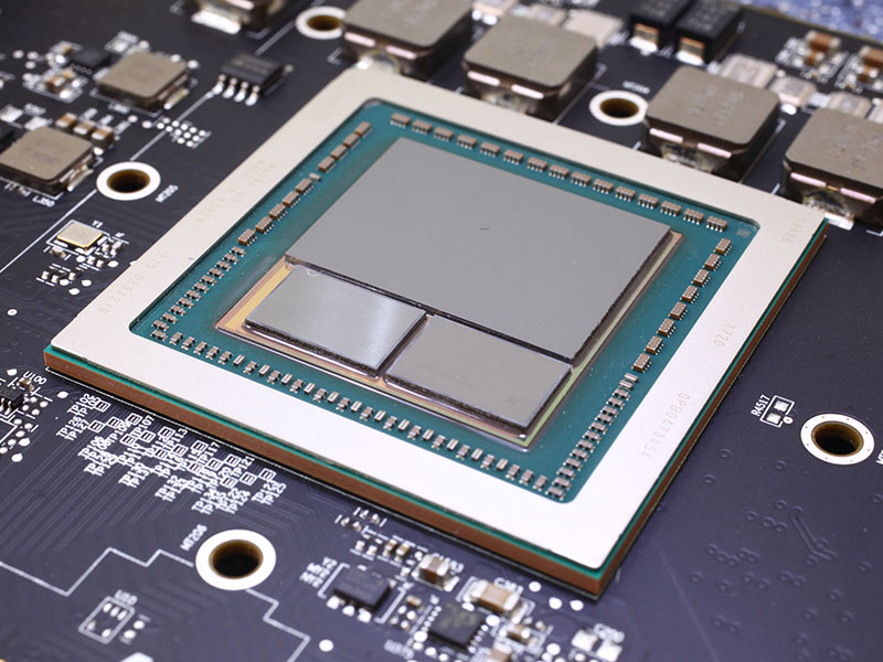
Chiplet + Interposer:
Multi-chip modules have existed for a very long time, and in the PC space Intel were doing something like that a long time before AMD were, e.g. the Pentium Pro (1995 - CPU and cache dies both on same ceramic package). What do you define as a chiplet exactly...? And for that matter the interposer is surely the ceramic package in this case:
1728581205794.jpeg


Other 'chiplet' / 'interposer' combinations pre-AM4:
PS3 RSX: View attachment 1728582406838.webp
Intel Pentium D:
1728580721239.jpeg


3D Stacking:
I'm afraid in the push for more NAND flash storage space for SSDs, Toshiba were ahead there:
1728581545604.jpeg


HDR:
You'd need to provide some specific example - dynamic range (and the lack of ability to recreate it on screen) has been well known for decades. There were many 'solutions' developed - I'm not sure what AMD brought to the table seeing as the 'modern' current take on it really is more along the lines of work done by Brightside/Dolby in terms of actual displays and standards, meanwhile game engines (even Valve's Source engine) were tackling HDR like capabilities through software approaches. Being first to support a standard others may have come up with isn't really a first in terms of developing that solution / standard.


On the other hand - things you didn't mention which people may attribute to Intel or AMD:
On-die memory controller - maybe not the first in terms of tech as many ARM devices for example use such a thing, but in the PC space AMD were first for consumers.
If it wasn't delayed, AMD would have had the first on-die full socketed 'northbridge' SoC with Llano / FM1 socket incorporating PCIe, IMC, and other bus connections directly to the CPU package... but it was late so Intel technically gets there with the LGA 1156.
But technically, these items themselves are really just a derivative of the 'Geode' line features conceptually speaking, which Cyrix (eeewwww) started.
 

Attachments

Last edited:

2017 AMD was using a silicon interposer.

As much hate/dislike/distain anyone may have they did a LOT first and have moved the needle for consumers.
Here are their firsts.

Tessellation
GPU compute
X64
Chiplet
Interposer
3D stacking
HBM
SSD on GPU
HDR


Intel was the pioneer of HT/SMT. They have made huge advances in paying off companies in monopolistic practices and been fined a pittance for trying to eliminate competitive companies. Nvidia has a great PR and spin team and a lot of money.

Intels Foveros directly connect two dies that are next to each other with no gap as in the AMD pic you posted.
 
Back
Top