- Joined
- Oct 9, 2007
- Messages
- 47,677 (7.43/day)
- Location
- Dublin, Ireland
| System Name | RBMK-1000 |
|---|---|
| Processor | AMD Ryzen 7 5700G |
| Motherboard | Gigabyte B550 AORUS Elite V2 |
| Cooling | DeepCool Gammax L240 V2 |
| Memory | 2x 16GB DDR4-3200 |
| Video Card(s) | Galax RTX 4070 Ti EX |
| Storage | Samsung 990 1TB |
| Display(s) | BenQ 1440p 60 Hz 27-inch |
| Case | Corsair Carbide 100R |
| Audio Device(s) | ASUS SupremeFX S1220A |
| Power Supply | Cooler Master MWE Gold 650W |
| Mouse | ASUS ROG Strix Impact |
| Keyboard | Gamdias Hermes E2 |
| Software | Windows 11 Pro |
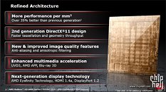
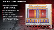
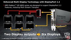
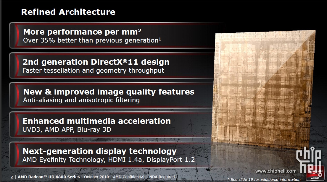
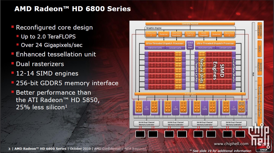
Specifications of the upcoming Radeon HD 6800 series GPUs have already been doing rounds for the last couple of days, and ChipHell.com finally managed to leak an alleged press-deck of the HD 6800 series that discloses the GPUs' specifications and some key features that AMD will introduce with this generation. What can be said looking at the slides is that AMD seems to have stepped up performance/die-size big time (up to 35% increase in performance per mm²), with some reconfiguring of key components. It also redesigned the GPUs to have up to 100% increase in tessellation performance, new image-quality enhancements, a new video acceleration engine (UVD 3), and a redesigned display IO with 2nd Gen. Eyefinity technology that can let users of standard variants drive up to six displays with a single card.
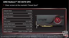
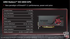
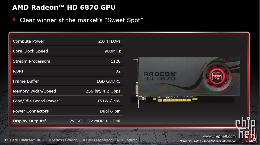
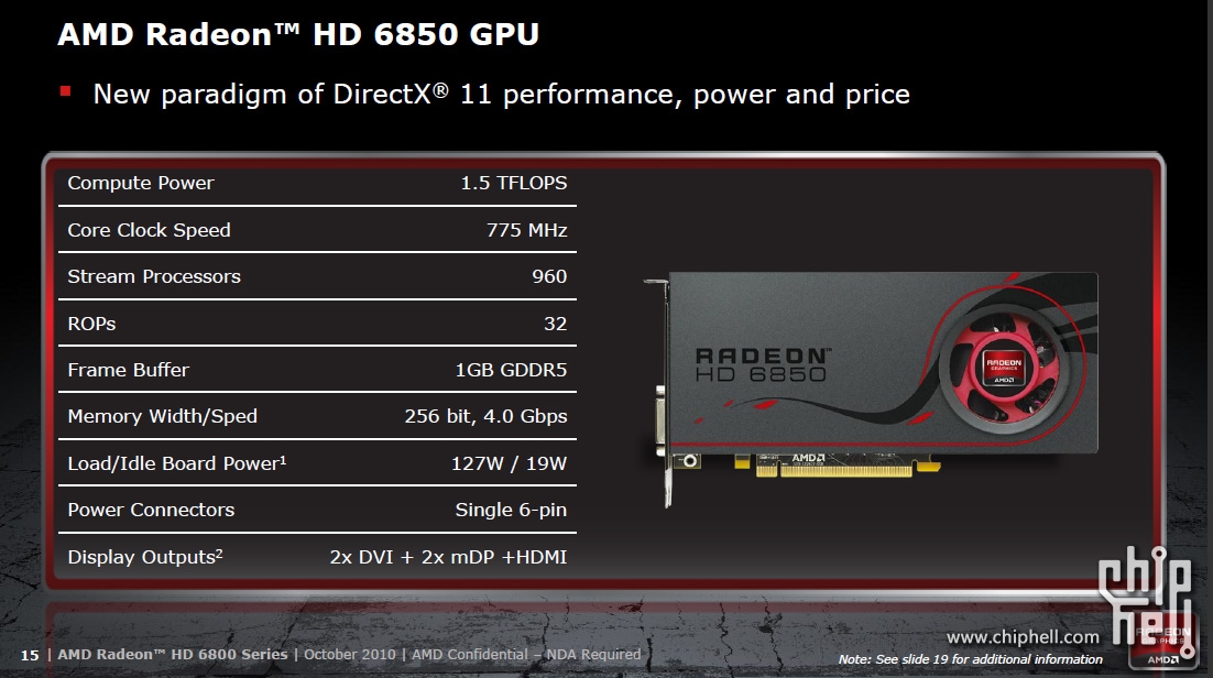
Specifications of the HD 6870 are: 1120 stream processors, 32 ROPs, 56 TMUs, 256-bit GDDR5 memory interface holding 1 GB, clock speeds of 900/1050(4200) MHz core/memory(effective), and idle/max board power of 19W/151W. For the HD 6850, it's 960 stream processors, 32 ROPs, 48 TMUs, 256-bit GDDR5 memory interface holding 1 GB, clock speeds of 775/1000(4000) MHz, idle/max board power of 19W/127W.
View at TechPowerUp Main Site
Specifications of the HD 6870 are: 1120 stream processors, 32 ROPs, 56 TMUs, 256-bit GDDR5 memory interface holding 1 GB, clock speeds of 900/1050(4200) MHz core/memory(effective), and idle/max board power of 19W/151W. For the HD 6850, it's 960 stream processors, 32 ROPs, 48 TMUs, 256-bit GDDR5 memory interface holding 1 GB, clock speeds of 775/1000(4000) MHz, idle/max board power of 19W/127W.

View at TechPowerUp Main Site


")


 ), shows seperate tesselator, etc...confirms 100% increase...ugh...this is exactly what i expected.
