- Joined
- Oct 9, 2007
- Messages
- 47,475 (7.50/day)
- Location
- Hyderabad, India
| System Name | RBMK-1000 |
|---|---|
| Processor | AMD Ryzen 7 5700G |
| Motherboard | ASUS ROG Strix B450-E Gaming |
| Cooling | DeepCool Gammax L240 V2 |
| Memory | 2x 8GB G.Skill Sniper X |
| Video Card(s) | Palit GeForce RTX 2080 SUPER GameRock |
| Storage | Western Digital Black NVMe 512GB |
| Display(s) | BenQ 1440p 60 Hz 27-inch |
| Case | Corsair Carbide 100R |
| Audio Device(s) | ASUS SupremeFX S1220A |
| Power Supply | Cooler Master MWE Gold 650W |
| Mouse | ASUS ROG Strix Impact |
| Keyboard | Gamdias Hermes E2 |
| Software | Windows 11 Pro |
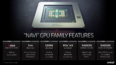
AMD "Navi 10" is a very different GPU from the "Vega 10," or indeed the "Polaris 10." The GPU sees the introduction of the new RDNA graphics architecture, which is the first big graphics architecture change on an AMD GPU in nearly a decade. AMD had in 2011 released its Graphics CoreNext (GCN) architecture, and successive generations of GPUs since then, brought generational improvements to GCN, all the way up to "Vega." At the heart of RDNA is its brand new Compute Unit (CU), which AMD redesigned to increase IPC, or single-thread performance.
Before diving deeper, it's important to confirm two key specifications of the "Navi 10" GPU. The ROP count of the silicon is 64, double that of the "Polaris 10" silicon, and same as "Vega 10." The silicon has sixteen render-backends (RBs), these are quad-pumped, which work out to an ROP count of 64. AMD also confirmed that the chip has 160 TMUs. These TMUs are redesigned to feature 64-bit bi-linear filtering. The Radeon RX 5700 XT maxes out the silicon, while the RX 5700 disables four RDNA CUs, working out to 144 TMUs. The ROP count on the RX 5700 is unchanged at 64.

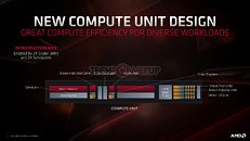
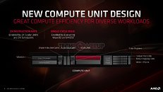
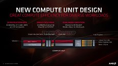
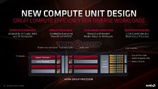
The RDNA Compute Unit sees the bulk of AMD's innovation. Groups of two CUs make a "Dual Compute Unit" that share a scalar data cahe, shader instruction cache, and a local data share. Each CU is now split between two SIMD units of 32 stream processors, a vector register, and a scalar unit, each. This way, AMD doubled the number of scalar units on the silicon to 80, double the CU count. Each scalar unit is similar in concept to a CPU core, and is designed to handle heavy scalar indivisible workloads. Each SIMD unit has its own scheduler. Four TMUs are part of each CU. This massive redesign in SIMD and CU hierarchy achieves a doubling in scalar- and vector instruction rates, and resource pooling between every two adjacent CUs.

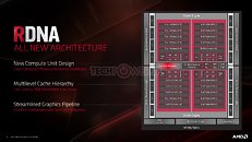
Groups of five RDNA dual-compute unit share a prim unit, a rasterizer, 16 ROPs, and a large L1 cache. Two such groups make a Shader Engine, and the two Shader Engines meet at a centralized Graphics Command Processor that marshals workloads between the various components, a Geometry Processor, and four Asynchronous-Compute Engines (ACEs).
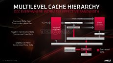
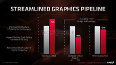
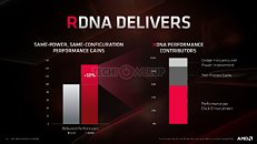
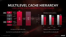
The second major redesign "Navi" features over previous generations is the cache hierarchy. Each RDNA dual-CU has a local fast cache AMD refers to as L0 (level zero). Each 16 KB L0 unit is made up of the fastest SRAM, and cushions direct transfers between the compute units and the L1 cache, bypassing the compute unit's I-cache and K-cache. The 128 KB L1 cache shared between five dual-CUs is a 16-way block of fast SRAM cushioning transfers between the shade engines and the 4 MB of L2 cache.
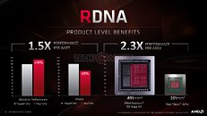
In all, RDNA helps AMD achieve a 2.3x gain in performance per area, 1.5x gain in performance per Watt. The "Navi 10" silicon measures just 251 mm² compared to the 495 mm² of the "Vega 10" GPU die. A lot of these spatial gains are also attributable to the switch to the new 7 nm silicon fabrication process from 14 nm.




AMD also briefly touched on its vision for real-time ray-tracing. To begin with, we can confirm that the "Navi 10" silicon has no fixed function hardware for ray-tracing such as the RT core or tensor cores found in NVIDIA "Turing" RTX GPUs. For now, AMD's implementation of DXR (DirectX Ray-tracing) for now relies entirely on programmable shaders. At launch the RX 5700 series won't be advertised to support DXR. AMD will instead release support through driver updates. The RDNA 2 architecture scheduled for 2020-21 will pack some fixed-function hardware for certain real-time ray-tracing effects. AMD sees a future in which real-time ray-tracing is handled on the cloud. The next frontier for cloud-computing is cloud-assist, where your machine can offload processing workloads to the cloud.
View at TechPowerUp Main Site
Before diving deeper, it's important to confirm two key specifications of the "Navi 10" GPU. The ROP count of the silicon is 64, double that of the "Polaris 10" silicon, and same as "Vega 10." The silicon has sixteen render-backends (RBs), these are quad-pumped, which work out to an ROP count of 64. AMD also confirmed that the chip has 160 TMUs. These TMUs are redesigned to feature 64-bit bi-linear filtering. The Radeon RX 5700 XT maxes out the silicon, while the RX 5700 disables four RDNA CUs, working out to 144 TMUs. The ROP count on the RX 5700 is unchanged at 64.


The RDNA Compute Unit sees the bulk of AMD's innovation. Groups of two CUs make a "Dual Compute Unit" that share a scalar data cahe, shader instruction cache, and a local data share. Each CU is now split between two SIMD units of 32 stream processors, a vector register, and a scalar unit, each. This way, AMD doubled the number of scalar units on the silicon to 80, double the CU count. Each scalar unit is similar in concept to a CPU core, and is designed to handle heavy scalar indivisible workloads. Each SIMD unit has its own scheduler. Four TMUs are part of each CU. This massive redesign in SIMD and CU hierarchy achieves a doubling in scalar- and vector instruction rates, and resource pooling between every two adjacent CUs.


Groups of five RDNA dual-compute unit share a prim unit, a rasterizer, 16 ROPs, and a large L1 cache. Two such groups make a Shader Engine, and the two Shader Engines meet at a centralized Graphics Command Processor that marshals workloads between the various components, a Geometry Processor, and four Asynchronous-Compute Engines (ACEs).


The second major redesign "Navi" features over previous generations is the cache hierarchy. Each RDNA dual-CU has a local fast cache AMD refers to as L0 (level zero). Each 16 KB L0 unit is made up of the fastest SRAM, and cushions direct transfers between the compute units and the L1 cache, bypassing the compute unit's I-cache and K-cache. The 128 KB L1 cache shared between five dual-CUs is a 16-way block of fast SRAM cushioning transfers between the shade engines and the 4 MB of L2 cache.
In all, RDNA helps AMD achieve a 2.3x gain in performance per area, 1.5x gain in performance per Watt. The "Navi 10" silicon measures just 251 mm² compared to the 495 mm² of the "Vega 10" GPU die. A lot of these spatial gains are also attributable to the switch to the new 7 nm silicon fabrication process from 14 nm.


AMD also briefly touched on its vision for real-time ray-tracing. To begin with, we can confirm that the "Navi 10" silicon has no fixed function hardware for ray-tracing such as the RT core or tensor cores found in NVIDIA "Turing" RTX GPUs. For now, AMD's implementation of DXR (DirectX Ray-tracing) for now relies entirely on programmable shaders. At launch the RX 5700 series won't be advertised to support DXR. AMD will instead release support through driver updates. The RDNA 2 architecture scheduled for 2020-21 will pack some fixed-function hardware for certain real-time ray-tracing effects. AMD sees a future in which real-time ray-tracing is handled on the cloud. The next frontier for cloud-computing is cloud-assist, where your machine can offload processing workloads to the cloud.
View at TechPowerUp Main Site


 (funny since the next Xbox and PS will have RT and they are not using Nivida for their GPU's ... well not that i care more for Consoles than i care about RT, tho)