- Joined
- Aug 19, 2017
- Messages
- 2,896 (1.04/day)
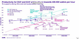
ASML, the world's sole provider of extreme ultraviolet (EUV) lithography systems essential for manufacturing the most advanced chips, has revealed its roadmap for pushing semiconductor scaling even further. In a recent presentation, former ASML president Martin van den Brink announced the company's plans for a new "Hyper-NA" EUV technology that would succeed the High-NA EUV systems, which are just beginning to deploy. The Hyper-NA tools, still in early research stages, would increase the numerical aperture to 0.75 from High-NA's 0.55, enabling chips with transistor densities beyond the projected limits of High-NA in the early 2030s. This higher numerical aperture should reduce reliance on multi-patterning techniques that add complexity and cost.
Hyper-NA is bringing challenges of its own to commercialization. Key obstacles include light polarization effects that degrade imaging contrast, requiring polarization filters that reduce light throughput. Resist materials may also need to become thinner to maintain resolution. While leading EUV chipmakers like TSMC can likely extend scaling for several more nodes using multi-patterning with existing 0.33 NA EUV tools, Intel has adopted 0.55 High-NA to avoid these complexities. But Hyper-NA will likely become essential across the industry later this decade as High-NA's physical limits are reached. Beyond Hyper-NA, few alternative patterning solutions exist besides expensive multi-beam electron lithography, which lacks the throughput of EUV photolithography. To continue classical scaling, the industry may need to eventually transition to new channel materials with superior electron mobility properties compared to silicon, requiring novel deposition and etch capabilities.


View at TechPowerUp Main Site | Source
Hyper-NA is bringing challenges of its own to commercialization. Key obstacles include light polarization effects that degrade imaging contrast, requiring polarization filters that reduce light throughput. Resist materials may also need to become thinner to maintain resolution. While leading EUV chipmakers like TSMC can likely extend scaling for several more nodes using multi-patterning with existing 0.33 NA EUV tools, Intel has adopted 0.55 High-NA to avoid these complexities. But Hyper-NA will likely become essential across the industry later this decade as High-NA's physical limits are reached. Beyond Hyper-NA, few alternative patterning solutions exist besides expensive multi-beam electron lithography, which lacks the throughput of EUV photolithography. To continue classical scaling, the industry may need to eventually transition to new channel materials with superior electron mobility properties compared to silicon, requiring novel deposition and etch capabilities.


View at TechPowerUp Main Site | Source


