- Joined
- May 21, 2024
- Messages
- 735 (3.42/day)
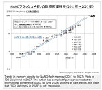
Kioxia presented a technology roadmap at the IWM 2024 conference in Seoul, projecting the development of 1,000-layer 3D NAND by 2027. This ambitious goal is based on extrapolating past trends, which saw NAND layers increase from 24 in 2014 to 238 in 2022. Kioxia's plan involves not only increasing layer count but also shrinking cell size and increasing bit levels from TLC (3 bits per cell) to QLC (4 bits per cell), and possibly even to PLC (5 bits per cell).
However, these advancements come with significant technical challenges. Etching the vertical connecting holes (through-silicon vias or TSVs) are harder to achieve and can lead to higher channel resistance. Kioxia proposes solutions such as using single-crystalline silicon instead of polysilicon and switching from tungsten to molybdenum to reduce resistance. They also suggest moving to multi-lane wordlines to reduce the die area needed for electrical connectivity.


While Kioxia focuses on technical solutions, their manufacturing partner Western Digital raises concerns about the economic viability of continued rapid advancement. Western Digital's EVP Robert Soderbery highlighted that 3D NAND requires higher capital intensity but delivers lower cost reduction as bit density increases. He suggested a slowdown in layer count increases to optimize capital deployment and extend the lifetime of each node level, Soderbery stated: "We're no longer on a hamster wheel of nodal migration.".
This difference in perspective could lead to tensions between Kioxia and Western Digital. While Kioxia aims to compete with industry leader Samsung by rapidly increasing layer counts, Western Digital appears more focused on maximizing returns on investment for each node level. This divergence may result in challenging discussions between the partners regarding the pace and timing of future NAND advancements.
View at TechPowerUp Main Site | Source
However, these advancements come with significant technical challenges. Etching the vertical connecting holes (through-silicon vias or TSVs) are harder to achieve and can lead to higher channel resistance. Kioxia proposes solutions such as using single-crystalline silicon instead of polysilicon and switching from tungsten to molybdenum to reduce resistance. They also suggest moving to multi-lane wordlines to reduce the die area needed for electrical connectivity.


While Kioxia focuses on technical solutions, their manufacturing partner Western Digital raises concerns about the economic viability of continued rapid advancement. Western Digital's EVP Robert Soderbery highlighted that 3D NAND requires higher capital intensity but delivers lower cost reduction as bit density increases. He suggested a slowdown in layer count increases to optimize capital deployment and extend the lifetime of each node level, Soderbery stated: "We're no longer on a hamster wheel of nodal migration.".
This difference in perspective could lead to tensions between Kioxia and Western Digital. While Kioxia aims to compete with industry leader Samsung by rapidly increasing layer counts, Western Digital appears more focused on maximizing returns on investment for each node level. This divergence may result in challenging discussions between the partners regarding the pace and timing of future NAND advancements.
View at TechPowerUp Main Site | Source


