- Joined
- Aug 19, 2017
- Messages
- 2,915 (1.05/day)
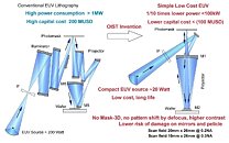
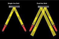
Japanese professor Tsumoru Shintake of the Okinawa Institute of Science and Technology (OIST) has unveiled a revolutionary extreme ultraviolet (EUV) lithography technology that promises to significantly push down semiconductor manufacturing costs. The new technology tackles two previously insurmountable issues in EUV lithography. First, it introduces a streamlined optical projection system using only two mirrors, a dramatic simplification from the conventional six or more. Second, it employs a novel "dual line field" method to efficiently direct EUV light onto the photomask without obstructing the optical path. Prof. Shintake's design offers substantial advantages over current EUV lithography machines. It can operate with smaller EUV light sources, consuming less than one-tenth of the power required by conventional systems. This reduction in energy consumption also reduces operating expenses (OpEx), which are usually high in semiconductor manufacturing facilities.
The simplified two-mirror design also promises improved stability and maintainability. While traditional EUV systems often require over 1 megawatt of power, the OIST model can achieve comparable results with just 100 kilowatts. Despite its simplicity, the system maintains high contrast and reduces mask 3D effects, which is crucial for attaining nanometer-scale precision in semiconductor production. OIST has filed a patent application for this technology, with plans for practical implementation through demonstration experiments. The global EUV lithography market is projected to grow from $8.9 billion in 2024 to $17.4 billion by 2030, when most nodes are expected to use EUV scanners. In contrast, ASML's single EUV scanner can cost up to $380 million without OpEx, which is very high thanks to the power consumption of high-energy light UV light emitters. Regular EUV scanners also lose 40% of the UV light going to the next mirror, with only 1% of the starting light source reaching the silicon wafer. And that is while consuming over one megawatt of power. However, with the proposed low-cost EUV system, more than 10% of the energy makes it to the wafer, and the new system is expected to use less than 100 kilowatts of power while carrying a cost of less than 100 million, a third from ASML's flagship.


View at TechPowerUp Main Site | Source
The simplified two-mirror design also promises improved stability and maintainability. While traditional EUV systems often require over 1 megawatt of power, the OIST model can achieve comparable results with just 100 kilowatts. Despite its simplicity, the system maintains high contrast and reduces mask 3D effects, which is crucial for attaining nanometer-scale precision in semiconductor production. OIST has filed a patent application for this technology, with plans for practical implementation through demonstration experiments. The global EUV lithography market is projected to grow from $8.9 billion in 2024 to $17.4 billion by 2030, when most nodes are expected to use EUV scanners. In contrast, ASML's single EUV scanner can cost up to $380 million without OpEx, which is very high thanks to the power consumption of high-energy light UV light emitters. Regular EUV scanners also lose 40% of the UV light going to the next mirror, with only 1% of the starting light source reaching the silicon wafer. And that is while consuming over one megawatt of power. However, with the proposed low-cost EUV system, more than 10% of the energy makes it to the wafer, and the new system is expected to use less than 100 kilowatts of power while carrying a cost of less than 100 million, a third from ASML's flagship.


View at TechPowerUp Main Site | Source


