• Welcome to TechPowerUp Forums, Guest! Please check out our forum guidelines for info related to our community.

Japanese Scientists Develop Less Complex EUV Scanners, Significantly Cutting Costs of Chip Development

AleksandarK

News Editor
Staff member
Joined
Aug 19, 2017
Messages
2,999 (1.07/day)
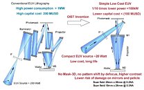
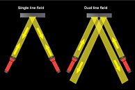
Japanese professor Tsumoru Shintake of the Okinawa Institute of Science and Technology (OIST) has unveiled a revolutionary extreme ultraviolet (EUV) lithography technology that promises to significantly push down semiconductor manufacturing costs. The new technology tackles two previously insurmountable issues in EUV lithography. First, it introduces a streamlined optical projection system using only two mirrors, a dramatic simplification from the conventional six or more. Second, it employs a novel "dual line field" method to efficiently direct EUV light onto the photomask without obstructing the optical path. Prof. Shintake's design offers substantial advantages over current EUV lithography machines. It can operate with smaller EUV light sources, consuming less than one-tenth of the power required by conventional systems. This reduction in energy consumption also reduces operating expenses (OpEx), which are usually high in semiconductor manufacturing facilities.

The simplified two-mirror design also promises improved stability and maintainability. While traditional EUV systems often require over 1 megawatt of power, the OIST model can achieve comparable results with just 100 kilowatts. Despite its simplicity, the system maintains high contrast and reduces mask 3D effects, which is crucial for attaining nanometer-scale precision in semiconductor production. OIST has filed a patent application for this technology, with plans for practical implementation through demonstration experiments. The global EUV lithography market is projected to grow from $8.9 billion in 2024 to $17.4 billion by 2030, when most nodes are expected to use EUV scanners. In contrast, ASML's single EUV scanner can cost up to $380 million without OpEx, which is very high thanks to the power consumption of high-energy light UV light emitters. Regular EUV scanners also lose 40% of the UV light going to the next mirror, with only 1% of the starting light source reaching the silicon wafer. And that is while consuming over one megawatt of power. However, with the proposed low-cost EUV system, more than 10% of the energy makes it to the wafer, and the new system is expected to use less than 100 kilowatts of power while carrying a cost of less than 100 million, a third from ASML's flagship.


View at TechPowerUp Main Site | Source
 
I know to little to understand what’s going on there but if they really made it so much less complex to get the job done asml can shut its doors
 
Wonder if this will allow anyone other than ASML to get EUV machines up and running.
 
7 nm to 3 nm is EUV so not necessarily a match for ASML's newest High-NA EUV, which begins from 2 nm. And ASML may well licence this off Japan to stay competitive in the future. After all, their existing designs rely on a USA licence.
 
I know to little to understand what’s going on there but if they really made it so much less complex to get the job done asml can shut its doors
It comes with serious tradeoffs, such as small reticle size. See the comments below the linked article at Tom's. I'm sure we'll soon learn more because this optical setup does seem quite revolutionary.
 
I am no expert but this looks like they have holes in the lens/mirrors but somehow there is no leakage?
 
I am no expert but this looks like they have holes in the lens/mirrors but somehow there is no leakage?
Astronomers have been using it for decades and have developed software to compensate for distortions so its probably ok
 
I have completely beginner knowledge regarding the machines' manufacturing for this processes, but the way the Capitalist World is advancing and anything consumable is being made I still feel that I must ask, is this really an evolution/advancement/improvement or rather a cheapening/enshitification of the process just to churn-out more dies with questionable lifetimes and limiting usefulness?
 
Last edited:
I have completely beginner knowledge regarding the machines' manufacturing for this processes, but I still feel the way the Capitalist World is advancing and anything consumable is being made I must ask, is this really an evolution/advancement/improvement or a cheapening/enshitification of the process just to churn-out more dies with questionable lifetimes and limiting usefulness?
As usual, its probably a bit of both.
 
Astronomers have been using it for decades and have developed software to compensate for distortions so its probably ok
If @Crackong sees the same that I see, some light goes straight through M1 and M2 without being reflected. Maybe it's negligible. Or maybe the designers will have to design chips with an empty area in the middle.
 
If @Crackong sees the same that I see, some light goes straight through M1 and M2 without being reflected. Maybe it's negligible. Or maybe the designers will have to design chips with an empty area in the middle.

My guess was the middle section of the beam isn't reflected here.
So the beam became a donut.
Then part of the photomask isn't getting any light.
After that M1 and M2 are shaped according to the donut size.
The final image should still be a donut.......

2345.jpg
 
My guess was the middle section of the beam isn't reflected here.
So the beam became a donut.
Then part of the photomask isn't getting any light.
After that M1 and M2 are shaped according to the donut size.
The final image should still be a donut.......

View attachment 357923
Newtonians and Cassegrains, and other reflecting optics don't quite work that way. You don't see the donut of the obstruction/mirror outline if you are in focus.

Though it does have a bit of negative impact to the resolution, compared to otherwise similar optical systems without the obstruction. Similar to how you don't see the primary mirror shape on JWST images but you do see the (actually quite beautiful, in a way) diffraction spikes.

Interesting developments, for sure.
I see.
Maybe like this?
It looks quite the same replacing the M2 with the photomask, but the Tertiary mirror here doesn't have a hole in the center.

main-qimg-c0f8abfe7449e97e282e852a479b7d7d.jpg
 
I see.
Maybe like this?
It looks quite the same replacing the M2 with the photomask, but the Tertiary mirror here doesn't have a hole in the center.

View attachment 357933
I'd guess the photomask would also have to be in focus to resolve the details. Might be helpful to think it as something in the centre of the fourth mirror of this telescope, but reflective.
 
Hopefully the tech will not be stole by Chinese, Taiwanese, Netherlanders or whatever....
The world needs to end ASML monopoly, hopefully the Japanese tech companies will pick this up.
 
Newtonians and Cassegrains, and other reflecting optics don't quite work that way. You don't see the donut of the obstruction/mirror outline if you are in focus.

Though it does have a bit of negative impact to the resolution, compared to otherwise similar optical systems without the obstruction. Similar to how you don't see the primary mirror shape on JWST images but you do see the (actually quite beautiful, in a way) diffraction spikes.
That's it. None of the mirrors are in focus. The only objects that are in focus are the photomask and the chip. Or the star and the image sensor if it's a telescope.
 
Back
Top