• Welcome to TechPowerUp Forums, Guest! Please check out our forum guidelines for info related to our community.

AMD Patents Chiplet-based GPU Design With Active Cache Bridge

Raevenlord

News Editor
Joined
Aug 12, 2016
Messages
3,755 (1.18/day)
Location
Portugal
System Name The Ryzening
Processor AMD Ryzen 9 5900X
Motherboard MSI X570 MAG TOMAHAWK
Cooling Lian Li Galahad 360mm AIO
Memory 32 GB G.Skill Trident Z F4-3733 (4x 8 GB)
Video Card(s) Gigabyte RTX 3070 Ti
Storage Boot: Transcend MTE220S 2TB, Kintson A2000 1TB, Seagate Firewolf Pro 14 TB
Display(s) Acer Nitro VG270UP (1440p 144 Hz IPS)
Case Lian Li O11DX Dynamic White
Audio Device(s) iFi Audio Zen DAC
Power Supply Seasonic Focus+ 750 W
Mouse Cooler Master Masterkeys Lite L
Keyboard Cooler Master Masterkeys Lite L
Software Windows 10 x64
AMD on April 1st published a new patent application that seems to show the way its chiplet GPU design is moving towards. Before you say it, it's a patent application; there's no possibility for an April Fool's joke on this sort of move. The new patent develops on AMD's previous one, which only featured a passive bridge connecting the different GPU chiplets and their processing resources. If you want to read a slightly deeper dive of sorts on what chiplets are and why they are important for the future of graphics (and computing in general), look to this article here on TPU.

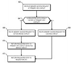
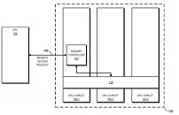
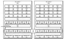
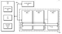
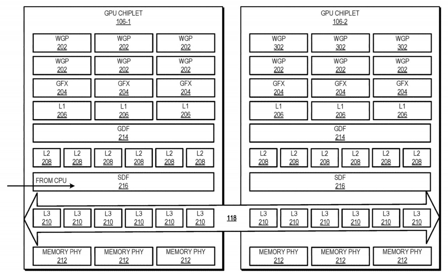
The new design interprets the active bridge connecting the chiplets as a last-level cache - think of it as L3, a unifying highway of data that is readily exposed to all the chiplets (in this patent, a three-chiplet design). It's essentially AMD's RDNA 2 Infinity Cache, though it's not only used as a cache here (and for good effect, if the Infinity Cache design on RDNA 2 and its performance uplift is anything to go by); it also serves as an active interconnect between the GPU chiplets that allow for the exchange and synchronization of information, whenever and however required. This also allows for the registry and cache to be exposed as a unified block for developers, abstracting them from having to program towards a system with a tri-way cache design. There are also of course yield benefits to be taken here, as there are with AMD's Zen chiplet designs, and the ability to scale up performance without any monolithic designs that are heavy in power requirements. The integrated, active cache bridge would also certainly help in reducing latency and maintaining chiplet processing coherency.


View at TechPowerUp Main Site
 
I'll pretend i understand this and just say "wooo progress!"
 
The cache hierarchy is already something that programmers do not have to deal with directly, that mechanism is hidden from you.

So more MH/s?
Not really, hashing algorithms are memory bound, so unless you increase the memory bandwidth it's not gonna matter how many chiplets there are.
 
At first glance I find it quite "challenging" to feed all cores with data, there will be scenario that GPU cores could "starve". But there is CPU access in the schematic, maybe as a command prefetcher or just DMA. AMD already has R-BAR so the CPU could play a big portion here.

-= edited=-
Remind me of hUMA, it all makes sense now why are they waiting to bring this to new AM5 platform with DDR5 RAM.
 
Last edited:
Not really, hashing algorithms are memory bound, so unless you increase the memory bandwidth it's not gonna matter how many chiplets there are.
Sure it matters. As long as AMD has a 4+GB caching chiplet it'll be awesome for mining :D
 
Oh, okay. I think I get it.

Infinitycache is Infinity Fabric for GPUs.

So rather than Infinity Fabric being a unified transport giving all CPU chiplets access to the memory controllers, Each GPU chiplet will have a baby/pseudo memory controller that seeds data into a massive shared L3 cache for all GPU chiplets too feed off.

Neat, probably. The move to chiplets will hurt overall IPC and efficiency slightly but it will move away from the single-biggest constraint GPUs have right now - manufacturing difficulties and yields on massive monolithic dies. You only have to look at the fact a 64C/128T Threadripper is available on a consumer/mainstream platform for the masses at $4000, whilst Intel is struggling so hard to get more than 24C in a processor that they'll charge $10-14K for the privilege and sell it only to server integrators as it's too much of a special snowflake to work in any non-proprietary mainstream platform using a regular, unified driver model.

AMD is shitting out 80mm² scalable chiplets at fantastic yields because of the small dies with 8C/16T and craploads of cache, whilst Intel's smallest 8C/16T part is 276mm² with zero scalability and half the cache.

Using the same silicon wafer yield calculator for both, AMD's gets ~696 sellable dies per wafer compared to Intel's ~161 sellable dies per wafer. Four times easier to make and the smaller die size also means that 92% of AMD's product is a flawless 8-core part, whilst around 25% of Intel's output needs to be harvested to make 6-core or worse.

So, if you take that example alone, GPU chiplets can't come soon enough.
 
Last edited:
Ravenlord said:
Before you say it, it's a patent application; there's no possibility for an April Fool's joke on this sort of move.

So this is a delayed April Fool Article? j/k :roll: :p

I expect the patent trolls are already digging for that one line of code or whatever so they can sue.

Infinitycache is Infinity Fabric for GPUs
not like they can use the same name, that serves, essentially, the same function.
 
not like they can use the same name, that serves, essentially, the same function.
That's what I was implying though, they're not the same function.
  • Infinity Fabric connects cores to memory controllers, and cores manage their cache.
  • Infinity cache connects cache to memory controllers, and cores manage their memory controllers.
I mean, sure - they both connect things which is the same function - but so do nails, tape, and string - yet those things are allowed to have different names? :p
 
So for those of you waiting for AMD to do to nVidia what they did to Intel....

Here it is.

Sounds like RDNA 3 will be an interesting generation for sure!
 
So more MH/s?
I dont think so. Look at the 6000 series. vs rtx 3000. rtx 3000 have higher memory bandwidth thats why they have more MH/S. Miners like memory speed vs Core speed
 
Oh, okay. I think I get it.

Infinitycache is Infinity Fabric for GPUs.

So rather than Infinity Fabric being a unified transport giving all CPU chiplets access to the memory controllers, Each GPU chiplet will have a baby/pseudo memory controller that seeds data into a massive shared L3 cache for all GPU chiplets too feed off.

Neat, probably. The move to chiplets will hurt overall IPC and efficiency slightly but it will move away from the single-biggest constraint GPUs have right now - manufacturing difficulties and yields on massive monolithic dies. You only have to look at the fact a 64C/128T Threadripper is available on a consumer/mainstream platform for the masses at $4000, whilst Intel is struggling so hard to get more than 24C in a processor that they'll charge $10-14K for the privilege and sell it only to server integrators as it's too much of a special snowflake to work in any non-proprietary mainstream platform using a regular, unified driver model.

AMD is shitting out 80mm² scalable chiplets at fantastic yields because of the small dies with 8C/16T and craploads of cache, whilst Intel's smallest 8C/16T part is 276mm² with zero scalability and half the cache.

Using the same silicon wafer yield calculator for both, AMD's gets ~696 sellable dies per wafer compared to Intel's ~161 sellable dies per wafer. Four times easier to make and the smaller die size also means that 92% of AMD's product is a flawless 8-core part, whilst around 25% of Intel's output needs to be harvested to make 6-core or worse.

So, if you take that example alone, GPU chiplets can't come soon enough.
hello yes i totally agree with your reasoning
 
The main issue with multicore/multithread/multi chips is how you get the modified data spread accross others chips. This is where the latency come from. The L3 cache in CPU is there for that specific roles.

Let say you modify some data. You will need to have the updated data available for other execution units. The easy way is to save it to ram, and them read it back but this add huge latency.

They use the L3 cache for that, this save a lot of time but when you have multiple L3 cache, you need to have mechanism that detect if the data is in another L3 cache and then collect it. (very simplified explanation)

Having it in the bridge is probably the best solution as it will be aware of all others chiplets. But, connecting that to each chiplets will add latency and will have reduced bandwidth. But chip design is all about compromise and making the best choice that give the best performance overall.

We will see
 
So more MH/s?
AMDs new cache for RDNA2 reduced mining performance and me thinks this one isn't one to help that type of workloads either...
 
I think AMD is going to leverage Infinity Cache to compete with Nvidia because they have been behind in the cache bandwidth race since Maxwell.
AMD had been successively expanding the chip resources, albeit never found the medium to express what it can do unequivocally.
 
I think AMD is going to leverage Infinity Cache to compete with Nvidia because they have been behind in the cache bandwidth race since Maxwell.
AMD had been successively expanding the chip resources, albeit never found the medium to express what it can do unequivocally.
Huh? Did you even read the OP? This is gpu chiplet.
 
The main issue with multicore/multithread/multi chips is how you get the modified data spread accross others chips. This is where the latency come from. The L3 cache in CPU is there for that specific roles.

Let say you modify some data. You will need to have the updated data available for other execution units. The easy way is to save it to ram, and them read it back but this add huge latency.
CPU cores often need to share data, GPU cores do not, what they need to execute is usually data independent.
 
I'll pretend i understand this and just say "wooo progress!"
The biggest issue with gpu chiplets like SLI are the developers. Thus they have to architect a way to do it seamlessly w/o relying on devs to make it work. And here we are one step closer.
 
The main issue with multicore/multithread/multi chips is how you get the modified data spread accross others chips. This is where the latency come from. The L3 cache in CPU is there for that specific roles.

Let say you modify some data. You will need to have the updated data available for other execution units. The easy way is to save it to ram, and them read it back but this add huge latency.

They use the L3 cache for that, this save a lot of time but when you have multiple L3 cache, you need to have mechanism that detect if the data is in another L3 cache and then collect it. (very simplified explanation)

Having it in the bridge is probably the best solution as it will be aware of all others chiplets. But, connecting that to each chiplets will add latency and will have reduced bandwidth. But chip design is all about compromise and making the best choice that give the best performance overall.

We will see
yes I also agree with you, but in my view this already comes from the first chips you remember the memories of 512KB or even 1MB were also very expensive and I think this will not change so soon unfortunately; hmm on the other hand is the price of constant evolution that we have to pay...
 
On one of the diagrams there’s an arrow going in from the CPU into the SDF. It appears the CPU will have direct access to the Scalable Data Fabric (which already makes up part of Infinity Fabric we see on Ryzen and Vega onwards GPUs) which will grant the ability of the CPU to read and write data to, from and between GPU chiplets thus connecting everything together. Which MAY allow for a more efficient and coherent data transfer between the CPU and GPU chiplets and between the GPU chiplets. The new (?maybe) interconnect within the GPU chiplet is the GDF lets call it Graphics Data Fabric which I dont know anything about yet which appears to offer all the WorkGroup Processors within the GPU chiplet coherency between them and the Level 2 cache. Interesting glimpse into the future.
 
CPU cores often need to share data, GPU cores do not, what they need to execute is usually data independent.
This is mostly true altought less and less true as there are more and more technique that reuse generated data. This is also why SLI/Crossfire is dead. The latency to move these data was just way too big. Temporal AA, ScreenSpace reflection, etc...
 
Oh, okay. I think I get it.

Infinitycache is Infinity Fabric for GPUs.

So rather than Infinity Fabric being a unified transport giving all CPU chiplets access to the memory controllers, Each GPU chiplet will have a baby/pseudo memory controller that seeds data into a massive shared L3 cache for all GPU chiplets too feed off.

Neat, probably. The move to chiplets will hurt overall IPC and efficiency slightly but it will move away from the single-biggest constraint GPUs have right now - manufacturing difficulties and yields on massive monolithic dies. You only have to look at the fact a 64C/128T Threadripper is available on a consumer/mainstream platform for the masses at $4000, whilst Intel is struggling so hard to get more than 24C in a processor that they'll charge $10-14K for the privilege and sell it only to server integrators as it's too much of a special snowflake to work in any non-proprietary mainstream platform using a regular, unified driver model.

AMD is shitting out 80mm² scalable chiplets at fantastic yields because of the small dies with 8C/16T and craploads of cache, whilst Intel's smallest 8C/16T part is 276mm² with zero scalability and half the cache.

Using the same silicon wafer yield calculator for both, AMD's gets ~696 sellable dies per wafer compared to Intel's ~161 sellable dies per wafer. Four times easier to make and the smaller die size also means that 92% of AMD's product is a flawless 8-core part, whilst around 25% of Intel's output needs to be harvested to make 6-core or worse.

So, if you take that example alone, GPU chiplets can't come soon enough.

Yes bouncing data around the dies will increase latency but that's easily mitigated by keeping data processing for each job within the die it's being worked on.
 
I mean, sure - they both connect things which is the same function - but so do nails, tape, and string - yet those things are allowed to have different names? :p
Kudos for the inverse pun - mentioning nails, tape and string but mysteriously leaving out glue.
 
Oh, okay. I think I get it.

Infinitycache is Infinity Fabric for GPUs.

So rather than Infinity Fabric being a unified transport giving all CPU chiplets access to the memory controllers, Each GPU chiplet will have a baby/pseudo memory controller that seeds data into a massive shared L3 cache for all GPU chiplets too feed off.

Neat, probably. The move to chiplets will hurt overall IPC and efficiency slightly but it will move away from the single-biggest constraint GPUs have right now - manufacturing difficulties and yields on massive monolithic dies. You only have to look at the fact a 64C/128T Threadripper is available on a consumer/mainstream platform for the masses at $4000, whilst Intel is struggling so hard to get more than 24C in a processor that they'll charge $10-14K for the privilege and sell it only to server integrators as it's too much of a special snowflake to work in any non-proprietary mainstream platform using a regular, unified driver model.

AMD is shitting out 80mm² scalable chiplets at fantastic yields because of the small dies with 8C/16T and craploads of cache, whilst Intel's smallest 8C/16T part is 276mm² with zero scalability and half the cache.

Using the same silicon wafer yield calculator for both, AMD's gets ~696 sellable dies per wafer compared to Intel's ~161 sellable dies per wafer. Four times easier to make and the smaller die size also means that 92% of AMD's product is a flawless 8-core part, whilst around 25% of Intel's output needs to be harvested to make 6-core or worse.

So, if you take that example alone, GPU chiplets can't come soon enough.
While I agree with most of your points, I so think your wrong on efficiency and IPC because people (Not AMD but scientists I can't recall including those of Nvidia)have already proven that it can be both more efficient and give higher IPC, forget people even, AMD themselves also proved it with the Zen architecture
 
Back
Top