- Joined
- Oct 9, 2007
- Messages
- 47,677 (7.43/day)
- Location
- Dublin, Ireland
| System Name | RBMK-1000 |
|---|---|
| Processor | AMD Ryzen 7 5700G |
| Motherboard | Gigabyte B550 AORUS Elite V2 |
| Cooling | DeepCool Gammax L240 V2 |
| Memory | 2x 16GB DDR4-3200 |
| Video Card(s) | Galax RTX 4070 Ti EX |
| Storage | Samsung 990 1TB |
| Display(s) | BenQ 1440p 60 Hz 27-inch |
| Case | Corsair Carbide 100R |
| Audio Device(s) | ASUS SupremeFX S1220A |
| Power Supply | Cooler Master MWE Gold 650W |
| Mouse | ASUS ROG Strix Impact |
| Keyboard | Gamdias Hermes E2 |
| Software | Windows 11 Pro |
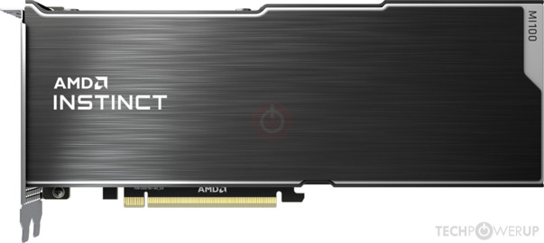
AMD's upcoming large post-Navi graphics chip, codenamed "Arcturus," will debut as "Radeon Instinct MI100", which is an AI-ML accelerator under the Radeon Instinct brand, which AMD calls "Server Accelerators." TechPowerUp accessed its BIOS, which is now up on our VGA BIOS database. The card goes with the device ID "0x1002 0x738C," which confirms "AMD" and "Arcturus,". The BIOS also confirms that memory size is at a massive 32 GB HBM2, clocked at 1000 MHz real (possibly 1 TB/s bandwidth, if memory bus width is 4096-bit).
Both Samsung (KHA884901X) and Hynix memory (H5VR64ESA8H) is supported, which is an important capability for AMD's supply chain. From the ID string "MI100 D34303 A1 XL 200W 32GB 1000m" we can derive that the TDP limit is set to a surprisingly low 200 W, especially considering this is a 128 CU / 8,192 shader count design. Vega 64 and Radeon Instinct MI60 for comparison have around 300 W power budget with 4,096 shaders, 5700 XT has 225 W with 2560 shaders, so either AMD achieved some monumental efficiency improvements with Arcturus or the whole design is intentionally running constrained, so that AMD doesn't reveal their hand to these partners, doing early testing of the card.
-- images removed --
Looking through the BIOS I also found what looks like several clock tables that top out at 1334 MHz, 1091 MHz, 1000 MHz. AMD's engineers typically list clocks in the following order: GPU clock, SOC clock, memory clock. This suggests that the GPU will tick at up to 1334 MHz, way lower than what Navi and Vega were able to achieve — maybe they do that to operate the chip in a more power-efficient way. The memory clock at 1000 MHz, matches the BIOS id string's "1000m", and falls in range with the 2.0 - 2.4 Gbps that Samsung is speccing their HBM2 memory chips at.
Arcturus' debut as a Radeon Instinct product follows the pattern of AMD debuting new big GPUs as low-volume/high-margin AI-ML accelerators first, followed by Radeon Pro and finally Radeon client graphics products. Arcturus is not "big Navi," rather it seems to be much closer to Vega than to Navi, which makes perfect sense given its target market. AMD's Linux sources mention "It's because Arcturus has not 3D engine", which could hint at what AMD did with this chip: take Vega and remove all 3D raster graphics ability, which shaves a few billion transistors off the silicon, freeing up space for more CUs. For gamers, AMD is planning a new line of Navi 20-series chips leveraging 7 nm EUV for launch throughout 2020. Various higher-ups at AMD, including its CEO, publicly hinted that a big client-segment GPU is in the works, and that the company is very much interested at taking another swing at premium 4K UHD gaming.
View at TechPowerUp Main Site


") this is impressive stuff AMD
this is impressive stuff AMD