- Joined
- Oct 9, 2007
- Messages
- 47,670 (7.43/day)
- Location
- Dublin, Ireland
| System Name | RBMK-1000 |
|---|---|
| Processor | AMD Ryzen 7 5700G |
| Motherboard | Gigabyte B550 AORUS Elite V2 |
| Cooling | DeepCool Gammax L240 V2 |
| Memory | 2x 16GB DDR4-3200 |
| Video Card(s) | Galax RTX 4070 Ti EX |
| Storage | Samsung 990 1TB |
| Display(s) | BenQ 1440p 60 Hz 27-inch |
| Case | Corsair Carbide 100R |
| Audio Device(s) | ASUS SupremeFX S1220A |
| Power Supply | Cooler Master MWE Gold 650W |
| Mouse | ASUS ROG Strix Impact |
| Keyboard | Gamdias Hermes E2 |
| Software | Windows 11 Pro |
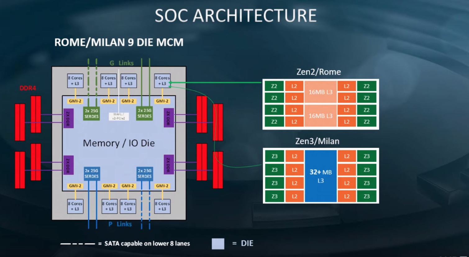
With its next-generation "Zen 3" CPU microarchitecture designed for the 7 nm EUV silicon fabrication process, AMD could bid the "Zen" compute complex or CCX farewell, heralding chiplets with monolithic last-level caches (L3 caches) that are shared across all cores on the chiplet. AMD embraced a quad-core compute complex approach to building multi-core processors with "Zen." At the time, the 8-core "Zeppelin" die featured two CCX with four cores, each. With "Zen 2," AMD reduced the CPU chiplet to only containing CPU cores, L3 cache, and an Infinity Fabric interface, talking to an I/O controller die elsewhere on the processor package. This reduces the economic or technical utility in retaining the CCX topology, which limits the amount of L3 cache individual cores can access.
This and more juicy details about "Zen 3" were put out by a leaked (later deleted) technical presentation by company CTO Mark Papermaster. On the EPYC side of things, AMD's design efforts will be spearheaded by the "Milan" multi-chip module, featuring up to 64 cores spread across eight 8-core chiplets. Papermaster talked about how the individual chiplets will feature "unified" 32 MB of last-level cache, which means a deprecation of the CCX topology. He also detailed an updated SMT implementation that doubles the number of logical processors per physical core. The I/O interface of "Milan" will retain PCI-Express gen 4.0 and eight-channel DDR4 memory interface.

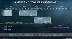
"Milan" is expected to see a Q3-2020 debut with EPYC. Around the same time, AMD tapes out "Genoa," the company's next-generation processor that heralds an all new enterprise socket dubbed SP5. A new socket gives AMD the opportunity to update and expand I/O such as increasing the memory interface width, add even more PCIe lanes, etc. The SP5 platform along with "Genoa" could see the light by 2021-22.
View at TechPowerUp Main Site
This and more juicy details about "Zen 3" were put out by a leaked (later deleted) technical presentation by company CTO Mark Papermaster. On the EPYC side of things, AMD's design efforts will be spearheaded by the "Milan" multi-chip module, featuring up to 64 cores spread across eight 8-core chiplets. Papermaster talked about how the individual chiplets will feature "unified" 32 MB of last-level cache, which means a deprecation of the CCX topology. He also detailed an updated SMT implementation that doubles the number of logical processors per physical core. The I/O interface of "Milan" will retain PCI-Express gen 4.0 and eight-channel DDR4 memory interface.
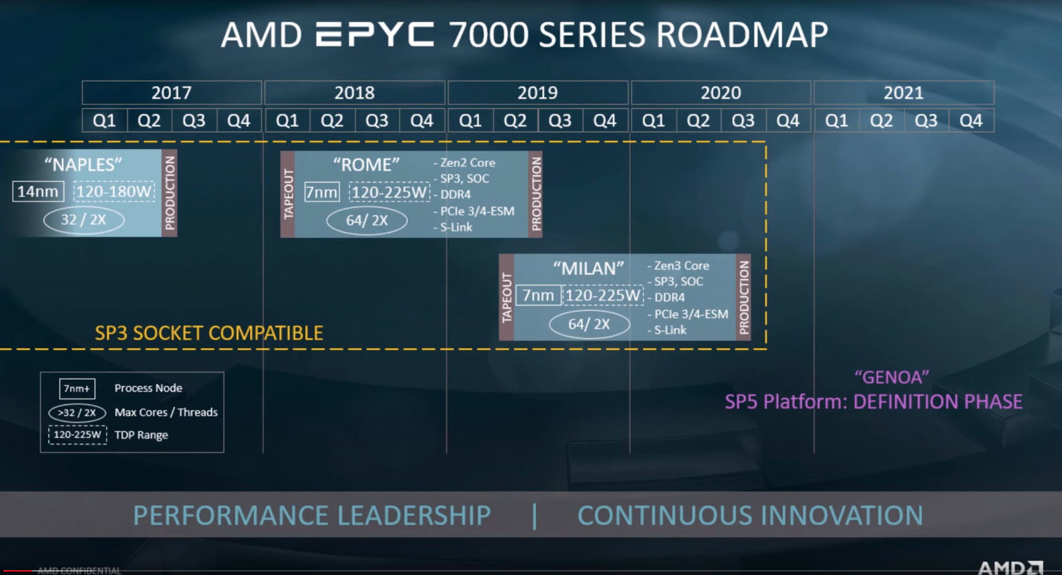
"Milan" is expected to see a Q3-2020 debut with EPYC. Around the same time, AMD tapes out "Genoa," the company's next-generation processor that heralds an all new enterprise socket dubbed SP5. A new socket gives AMD the opportunity to update and expand I/O such as increasing the memory interface width, add even more PCIe lanes, etc. The SP5 platform along with "Genoa" could see the light by 2021-22.
View at TechPowerUp Main Site


") Obviously seeing some Cinebench runs of it will make or break me buying something... (I jest) Reviews will let me know whether or not it's going to suck or be like most of AMDs recent reviews, to rave about
Obviously seeing some Cinebench runs of it will make or break me buying something... (I jest) Reviews will let me know whether or not it's going to suck or be like most of AMDs recent reviews, to rave about 
