• Welcome to TechPowerUp Forums, Guest! Please check out our forum guidelines for info related to our community.

Cost-Effective Radeon HD 7900 PCB Already In The Works

btarunr

Editor & Senior Moderator
Staff member
Joined
Oct 9, 2007
Messages
47,675 (7.43/day)
Location
Dublin, Ireland
System Name RBMK-1000
Processor AMD Ryzen 7 5700G
Motherboard Gigabyte B550 AORUS Elite V2
Cooling DeepCool Gammax L240 V2
Memory 2x 16GB DDR4-3200
Video Card(s) Galax RTX 4070 Ti EX
Storage Samsung 990 1TB
Display(s) BenQ 1440p 60 Hz 27-inch
Case Corsair Carbide 100R
Audio Device(s) ASUS SupremeFX S1220A
Power Supply Cooler Master MWE Gold 650W
Mouse ASUS ROG Strix Impact
Keyboard Gamdias Hermes E2
Software Windows 11 Pro
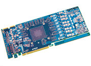
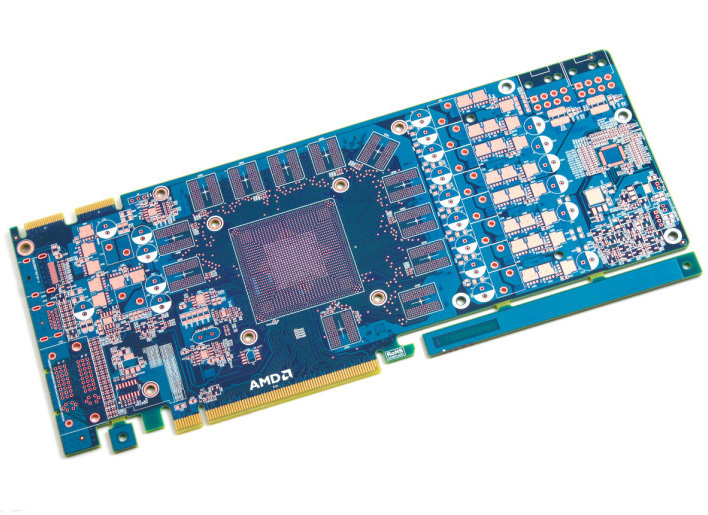
A little earlier today, we showed you pictures of AMD's first Radeon HD 7900 series single-GPU PCB that makes use of digital-PWM power delivery. Some of the first batches of Radeon HD 7900 graphics cards will stick to that PCB and board design, as it's backed by AMD's engineering. Even as the SKU's launch is less than 24 hours away, there are pictures of AMD's cost-effective Radeon HD 7900 PCB surfacing on Asian media sites. Once ready, AMD add-in board partners can opt for this cost-effective PCB if they want to fine-tune their prices. It looks like AMD is ready well ahead to face competition from NVIDIA, with its GeForce Kepler 104 (GK104) GPU.

The cost-effective PCB, without any components laid, is pictured below. The first picture shows its obverse side, the second, its reverse side. The PCB is completely up to speed with everything Tahiti GPU will need. It has provision for two 8-pin PCIe power inputs, an 8+2 phase cost-effective analog VRM, probably driven by a cost-effective CHIL controller, and a different display output connector loadout. It has provision for two DVI, and one each of HDMI and full-size DisplayPort. Partners can still use a single DVI connector, and keep their cards single-slot capable. Provisions for 12 GDDR5 chips are right where they should be. There is nothing eventful in the reverse side, just traces for all the supportive components.


View at TechPowerUp Main Site
 
FAQ #1: What is this?:

bta9874d.jpg


Ans: It's a spacer for the production line. They remove it after the assembly and QA are over. Your graphics card will have marks of its spacer if you look closely.
 
I see Yeston on one of the Images, It looks like it might be a Chinese marketed board version.
 
This PCB seems to make better use of space than the reference board than anything else.
 
I see Yeston on one of the Images, It looks like it might be a Chinese marketed board version.

The PCB has AMD brand markings on it. Yeston can't design its own PCB and use AMD markings on it. So it's a picture of a PCB designed by AMD, and not a "Chinese marketed board version."
 
FAQ #1: What is this?:

http://img.techpowerup.org/111221/bta9874d.jpg

Ans: It's a spacer for the production line. They remove it after the assembly and QA are over. Your graphics card will have marks of its spacer if you look closely.

Looks like something for machinery to hold onto during the manufacturing process. Pretty much looks like it snaps off. I only say this because there is another small tab toward the "front" of the PCB with a similar hole location to the long one at the "back".
 
Looks like something for machinery to hold onto during the manufacturing process. Pretty much looks like it snaps off.
They do snap it off at the end of production, and it is on the same place as most GPUs are, next to the PCI-E connector.
 
Looks like something for machinery to hold onto during the manufacturing process. Pretty much looks like it snaps off.

Yup. I made it a point to make that post to save a few dozen "OMG what is that ugly thing, it won't fit in my case/motherboard, AMD faaail" posts.
 
Yup. I made it a point to make that post to save a few dozen "OMG what is that ugly thing, it won't fit in my case/motherboard, AMD faaail" posts.

I was trolled very, very softly....

/kiss
 
The PCB has AMD brand markings on it. Yeston can't design its own PCB and use AMD markings on it. So it's a picture of a PCB designed by AMD, and not a "Chinese marketed board version."

So explain why Yeston had the Image when Yeston is an AIB of AMD then fyi, and if you look at other AIBs the PCB has AMD on the edge of it aswell.:shadedshu
 
So explain why Yeston had the Image when Yeston is an AIB of AMD then fyi, and if you look at other AIBs the PCB has AMD on the edge of it aswell.:shadedshu

I don't understand what is your argument exactly. You're arguing for the heck of it, over a total non-issue.
 
im just sayin the PCB design maybe for markets in Asia mainly. And Btarunr i wasnt arguing with you at all, just putting my thoughts in is all
 
im just sayin the PCB design maybe for markets in Asia mainly. And Btarunr i wasnt arguing with you at all, just putting my thoughts in is all

No, that PCB was designed by AMD. The Yeston watermark over an image is irrelevant. AMD designed a similar cost-effective reference PCB for Cayman (HD 6900 series GPU), which is sold everywhere, including the US, by pretty much every AIB. So this is not a China-specific PCB design.
 
Given the color scheme and being made by Yeston, this will most likely show up as Sapphire or HIS cards.
 
No, that PCB was designed by AMD. The Yeston watermark over an image is irrelevant. AMD designed a similar cost-effective reference PCB for Cayman (HD 6900 series GPU), which is sold everywhere, including the US, by pretty much every AIB. So this is not a China-specific PCB design.

which in turn the company Yeston will probably use the cost effective PCB for their Radeon lineup
 
Anyway back on topic looks like it may have 2 DVI connectors (no single slot solution)
 
Anyway back on topic looks like it may have 2 DVI connectors (no single slot solution)

its a modular design, as we head further into the future VGA and DVI are becoming less common as its being replaced by HDMI/mHDMI and Display Port, HDMI and DVI are interchangeable with an adapter, HDMI is practically DVI with the capability of transmitting Audio over the same connector.

This right here means board partners can have 1 or 2 dvi connectors and the rest HDMI/Display port, some boards will definitly be single slot and others will be dual slot
 
First of all even reference PCB has some chippo PWM. Don't know if it is digital, but needs heavy-duty capacitors, so it's output voltage ripple is high and needs smoothing. How is that better than ATI/AMD previous 3 generation? No 12 layer, 4 ounce gold PCB either. Who da fu*k came up with that ridiculously high prices :slap:
 
What is the difference between 8+2 phase cost-effective VRM and 5+1+1 VRM?
 
so this should be for 7950?
I think I've read that 7970 will all be stock while on 7950 AMD has given freedom to partners to clock / design cards as they want
 
Last edited:
FAQ #1: What is this?:
http://img.techpowerup.org/111221/bta9874d.jpg
Ans: It's a spacer for the production line. They remove it after the assembly and QA are over. Your graphics card will have marks of its spacer if you look closely.

Sometimes it's also because components are made "2 at a time" and then broken apart later like the ones in this vid. Of course you know that bta, just a message for the masses :p
 
To date, I've never seen a board more evenly spaced and clean. So far the HD 7900 series is looking good. Now for some benchmarks and how much warranty will be offered.

Reason I ask is because Western Digital along with its competition both have greatly reduced warranty for their hard drives due to the fact they are breaking down more often now. I find this counterproductive; if you are not capable of backing up your products, then get the hell out of dodge. HD 7900 series better have at least 3 years of warranty, better yet lifetime.
 
I agree with you about more warranty but atleast for me 3 years is more than I would keep a graphics card... I'd like more the warranty that covers heatsink removal
 
Back
Top